ML674001 Ver la hoja de datos (PDF) - Oki Electric Industry
Número de pieza
componentes Descripción
Fabricante
ML674001 Datasheet PDF : 24 Pages
| |||
OKI Semiconductor
FEDL674001-01
ML674001/67Q4002/67Q4003
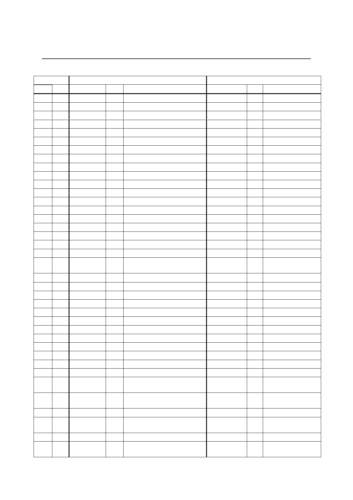
Pin
LQFP BGA Symbol
41
L4 VDD_IO
42 M3 XA[10]
43 N4 XA[11]
44
L5 XA[12]
45 M4 XA[13]
46 N5 XA[14]
47 K5 GND
48 M5 XA[15]
49 N6 XA[16]
50 M6 XA[17]
51 K6 GND
52
L6 XA[18]
53 M7 PIOC[2]
54 K7 VDD_IO
55
L7 PIOC[3]
56 N7 PIOC[4]
57
L8 PIOC[5]
58 K8 VDD_CORE
59 M8 PIOC[6]
60 M9 PIOC[7]
61 N8 XOE_N
62 K9 VDD_IO
63 M10 XWE_N
64 N9 XBWE_N[0]
65
L9 XBWE_N[1]
66 L10 XROMCS_N
67 N10 XRAMCS_N
68 M11 XIOCS_N[0]
69 K10 GND
70 N11 XIOCS_N[1]
71 M12 XIOCS_N[2]
72 N12 XIOCS_N[3]
73 N13 PIOD[6]
74 M13 PIOD[7]
75 L11 PIOB[0]
76 L13 PIOB[1]
77 K11 VDD_IO
78 L12 PIOB[2]
Primary Function
I/O
Description
VDD I/O power supply
O External address output
O External address output
O External address output
O External address output
O External address output
GND GND
O External address output
O External address output
O External address output
GND GND
O External address output
I/O General port (with interrupt function)
VDD I/O power supply
I/O General port (with interrupt function)
I/O General port (with interrupt function)
I/O General port (with interrupt function)
VDD CORE power supply
I/O General port (with interrupt function)
I/O General port (with interrupt function)
O
VDD
O
O
O
O
O
O
GND
O
O
O
I/O
Output enable (excluding SDRAM)
I/O power supply
Write enable
Byte write enable (LSB)
Byte write enable (MSB)
External ROM chip select
External RAM chip select
IO chip select 0
GND
IO chip select 1
IO chip select 2
IO chip select 3
General port (with interrupt function)
I/O General port (with interrupt function)
I/O General port (with interrupt function)
I/O General port (with interrupt function)
VDD I/O power supply
I/O General port (with interrupt function)
Secondary Function
Symbol
I/O
Description
—
—
—
—
—
—
—
—
—
—
—
—
—
—
—
—
—
—
—
—
—
—
—
—
XA[19]
O External address output
—
—
XA[20]
O External address output
XA[21]
O External address output
XA[22]
O External address output
—
—
XA[23]
O External address output
XWR
O Transfer direction of
external bus
—
—
—
—
—
—
—
—
—
—
—
—
—
—
—
—
—
—
—
—
—
—
—
—
XDQM[1]/XCAS O INPUT/OUTPUT
_N[1]
mask/CAS (MSB)
XDQM[0]/XCAS O INPUT/OUTPUT
_N[0]
mask/CAS (LSB)
DREQ[0]
I DMA request signal (CH0)
DREQCLR[0]
O DREQ Clear Signal
(CH0)
—
—
DREQ[1]
I DMA request signal
(CH1)
7/24
Share Link: 