ML4771 Ver la hoja de datos (PDF) - Micro Linear Corporation
Número de pieza
componentes Descripción
Fabricante
ML4771 Datasheet PDF : 8 Pages
| |||
DESIGN CONSIDERATIONS (Continued)
INPUT CAPACITOR
Due to the high input current drawn at startup and
possibly during operation, it is recommended to decouple
the input with a capacitor with a value of 47µF to 100µF.
This filtering prevents the input ripple from affecting the
ML4771 control circuitry, and also improves the efficiency
by reducing the I squared R losses during the charge cycle
of the inductor. Again, a low ESR capacitor (such as
tantalum) is recommended.
It is also recommended that low source impedance
batteries be used. Otherwise, the voltage drop across the
source impedance during high input current situations will
cause the ML4771 to fail to start-up or to operate
unreliably. In general, for two cell applications the source
impedance should be less than 200mW, which means that
small alkaline cells should be avoided.
SETTING THE OUTPUT VOLTAGE
The adjustable output of the ML4771 requires an external
feedback resistor divider to set VOUT. The output voltage
can be determined from the following equation:
1 6 VOUT
= 2.57
R1 + R2
R2
(3)
where R1 and R2 are connected as shown in Figure 2. The
value of R2 should be 250kW or less to minimize bias
current errors. Choose an appropriate value for R2 and
calculate R1.
LAYOUT
Good layout practices will ensure the proper operation of
the ML4771. Some layout guidelines follow:
• Use adequate ground and power traces or planes
• Keep components as close as possible to the ML4771
• Use short trace lengths from the inductor to the VL1 and
VL2 pins and from the output capacitor to the VOUT pin
• Use a single point ground for the ML4771 ground pin,
and the input and output capacitors
• Separate the ground for the converter circuitry from the
ground of the load circuitry and connect at a single
point
A sample layout is shown in Figure 7.
ML4771
DESIGN EXAMPLE
In order to design a boost converter using the ML4871, it
is necessary to define a few parameters. For this example,
assume that VIN = 3.0V to 3.6V, VOUT = 5.0V, and
IOUT(MAX) = 500mA.
First, it must be determined whether the ML4871 is
capable of delivering the output current. This is done using
Equation 1:
IOUT(MAX) = 1.25
3.0V
5.0V
0.7A = 0.53A
Next, select an inductor. As previously mentioned, the
recommended inductance is 10µH. Make sure that the
peak current rating of the inductor is at least 1.5A, and
that the DC resistance of the inductor is in the range of 50
to 100mW.
Then, the value of the output capacitor is determined
using Equation 2:
COUT
=
44 10mH
5.0V
=
88mF
The closest standard value would be a 100µF capacitor
with an ESR rating of 100mW. If such a low ESR value
cannot be found, two 47µF capacitors in parallel could
also be used.
Finally, the values of R1 and R2 are calculated using
equation 3, assuming that R2 = 250kW:
R1 =
5.0 250kW
2.57
- 250kW = 236kW
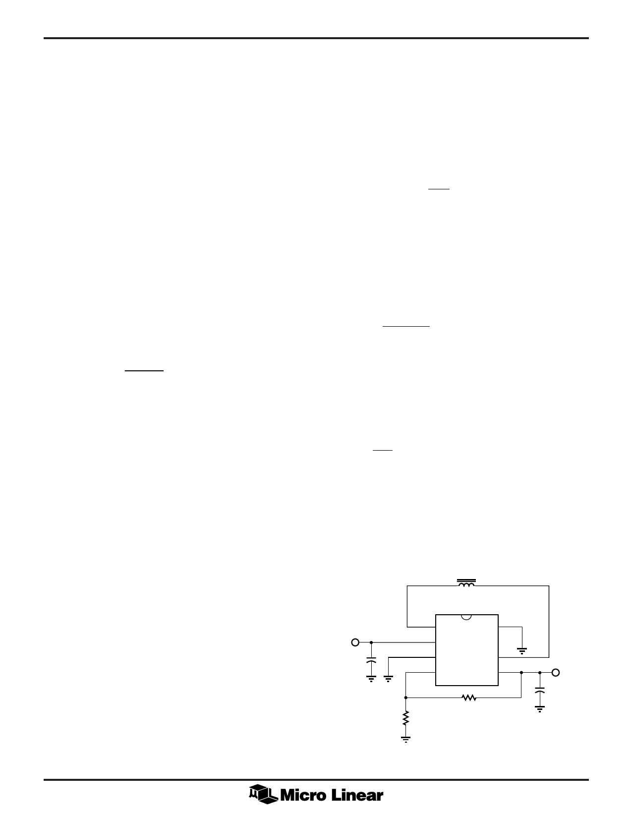
The complete circuit is shown in Figure 8. As mentioned
previously, the use of an input supply bypass capacitor is
highly recommended.
VIN
100µF
250kΩ
10µH
(Sumida CD75)
ML4771
VL1 PWR GND
VIN
NC
GND
VL2
SENSE VOUT
236kΩ
VOUT
100µF
Figure 8. Typical Application Circuit
7
Share Link: 