ML2500BTA Ver la hoja de datos (PDF) - Oki Electric Industry
Número de pieza
componentes Descripción
Fabricante
ML2500BTA
Oki Electric Industry

ML2500BTA Datasheet PDF : 27 Pages
| |||
OKI Semiconductor
FEDL2500BFULL-02
ML2500BTA
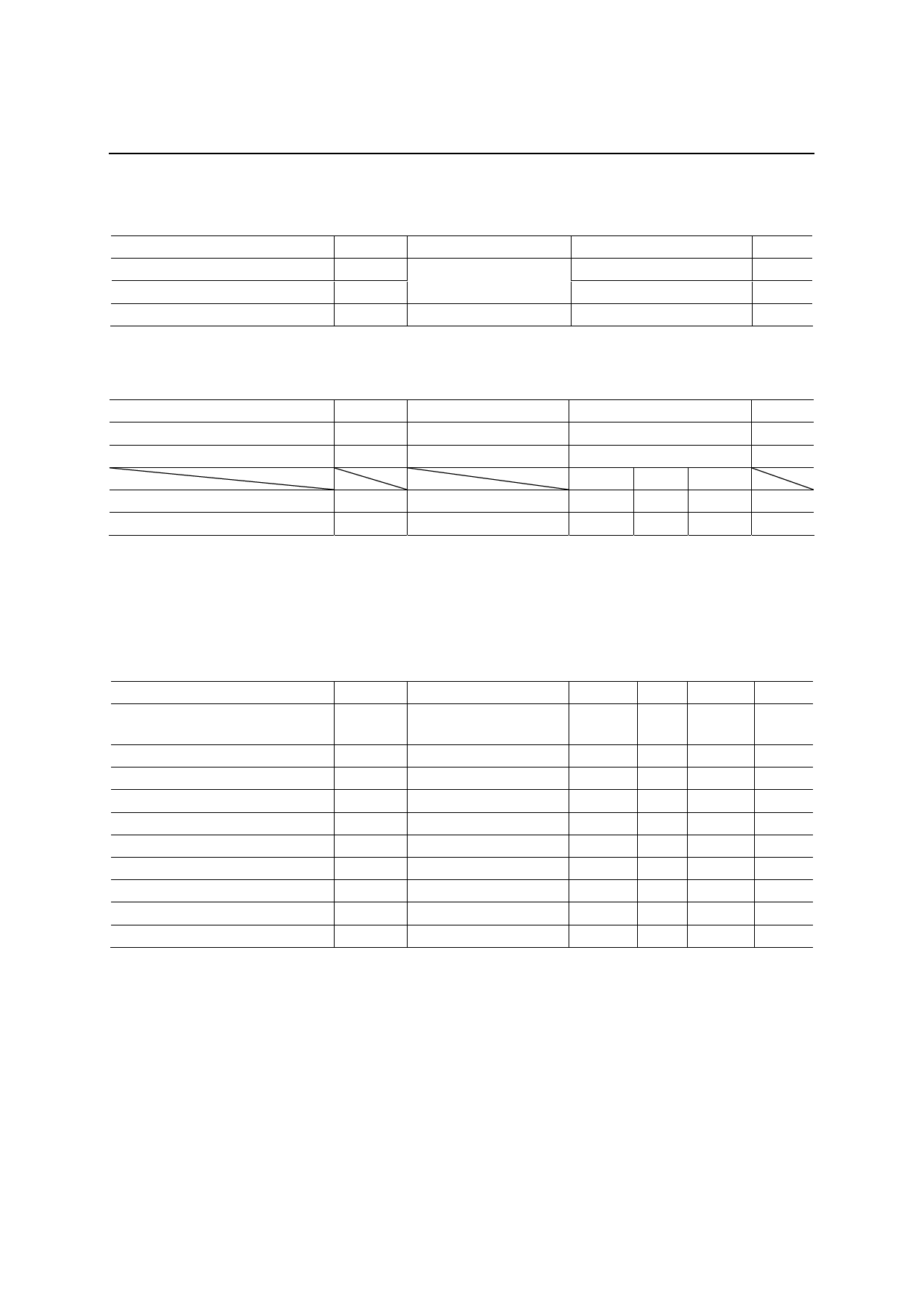
ABSOLUTE MAXIMUM RATINGS
Parameter
Power Supply Voltage
Input Voltage
Storage Temperature
Symbol
VDD
VIN
TSTG
Condition
Ta = 25°C
—
Rating
Unit
–0.3 to +5.0
V
–0.3 to VDD+0.3
V
–55 to +150
°C
RECOMMENDED OPERATING CONDITIONS
Parameter
Power Supply Voltage
Operating Temperature
Symbol
VDD
Top
Condition
DGND = AGND = 0 V
—
External Clock Frequency 1 *1 fEXTCLK1
—
External Clock Frequency 2 *1 fEXTCLK2
—
*1: Applicable only with external clock
Range
2.7 to 3.3
–40 to +70
Min. Typ. Max.
3.85 4.096 4.34
7.70 8.192 8.68
Unit
V
°C
MHz
MHz
ELECTRICAL CHARACTERISTICS
DC Characteristics
Parameter
“H” Input Voltage
*1
“L” Input Voltage
*1
“H” Output Voltage
*2
“L” Output Voltage
*2
“H” Input Current
*1
“L” Input Current
*1
Operating Current Consumption 1
Operating Current Consumption 2
Operating Current Consumption 3
Powerdown Current Consumption
DVDD = AVDD = 2.7 to 3.3 V, DGND = AGND = 0 V, Ta = –40 to +70°C
Symbol
Condition
Min. Typ. Max. Unit
0.8 ×
VIH
DGND = AGND = 0 V
VDD
—
—
V
VIL
—
—
— 0.2 × VDD V
VOH
lOH = –40 µA
VDD–0.3 —
—
V
VOL
lOL = 2 mA
—
—
0.45
V
IIH
VIH = VDD
—
—
10
µA
IIL
VIL = 0 V
–10
—
—
µA
IDD1
In Recording Operation
—
30
45
mA
IDD2
In Playback Operation
—
20
30
mA
IDD3 In Command-Wait State —
5
10
mA
IDDS
—
—
—
10
µA
*1: Applied to logic input pins (DI, SCK, CS, RESET and EXTCLK) except ROSC and TEST1 pins.
*2: Applied to logic output pins (DO and MON) except TEST2 pin.
5/27
Share Link: