MICRF008(2008) Ver la hoja de datos (PDF) - Micrel
NĂșmero de pieza
componentes DescripciĂłn
Fabricante
MICRF008 Datasheet PDF : 13 Pages
| |||
Micrel, Inc.
proportional to REFOSC frequency. The nominal value
of RSC given in the âElectrical Characteristics â Table is
220k⊠for a REFOSC frequency of 3.36MHz. Slicing
level time constant value vary depending on data
pattern, data rate and data duty cycle.
Automatic Gain Control (AGC)
The signal path has automatic gain control (AGC) to
increase the overall receiver dynamic range. An external
capacitor, CAGC, must be connected to the CAGC pin of
the device. Normally the CAGC capacitor is connected
to ground. If faster start-up times are required when the
receiver is first poweredon, the CAGC capacitor may be
connected to VDD. The ratio of decay-to-attack time
constant is fixed at 10:1 (that is, the attack time constant
is 1/10th of the decay time constant), and the user
cannot change this ratio. Nevertheless, the attack time
constant is set externally by choosing a value for CAGC.
Another function of the AGC control voltage is to raise
the noise floor in order to guarantee a clean signal
between the preamble and the data, sometimes called
dead time. The AGC control voltage can be further
manipulated and amplified to create an RSSI signal,
which is useful for several different applications.
Reference Oscillator
All timing and tuning operations on the MICRF008YM
are derived from the internal Colpitts reference oscillator.
The reference frequency can be implemented in two
ways, by using a resonator device (a ceramic resonator
or crystal), or by driving an external signal, which should
not exceed 0.5VRMS. The reference frequency is
obtained by dividing the RF carrier frequency by 129.
I/O Pin Interface Circuitry
Interface circuitry for the various I/O pins of the
MICRF008 is shown in Figures 2 through 6. Specific
information regarding each of these circuits is discussed
in the following subparagraphs. Not shown are ESD
protection diodes which are applied to all input pins.
CTH Pin
Figure 2 illustrates the CTH pin interface circuit. CTH pin
is driven from a P-Channel MOSFET source-follower
biased with approximately 20ÎŒA of bias current.
Transmission gates TG1 and TG2 isolate the 3.3pF
capacitor. Internal control signals PHI1/PHI2 are related
in a manner such that the impedance across the
transmission gates looks like a âresistance.â The DC
potential on the CTH pin is approximately 2.2V,
fundamentally determined by the VGS of the two
PChannel MOSFET source-followers shown.
MICRF008
VDDBB
20”A
VDDBB
20”A
Demod
Signal
(0Vdc)
DC-coupled
Switched
Cap. Filter
VSSBB
VSSBB
PHI2B
PHI1B
TG1
TG2
PHI2
3.3pF
PHI1
VSSBB
Figure 2. CTH Pin
CTH
CAGC Pin
Figure 3 illustrates the CAGC pin interface circuit. The
AGC control voltage is developed as an integrated
current into a capacitor CAGC. The attack current is
nominally 15ÎŒA, while the decay current is a 1/10th
scaling of this, approximately 1.5ÎŒA. Signal gain of the
RF/IF strip inside the IC diminishes as the voltage on
CAGC decreases. By simply adding a capacitor to
CAGC pin, the attack/decay time constant ratio is fixed
at 1:10.
VDDBB
1.5”A
Compa-
rator
CAGC
15”A
VSSBB
Figure 3. CAGC Pin
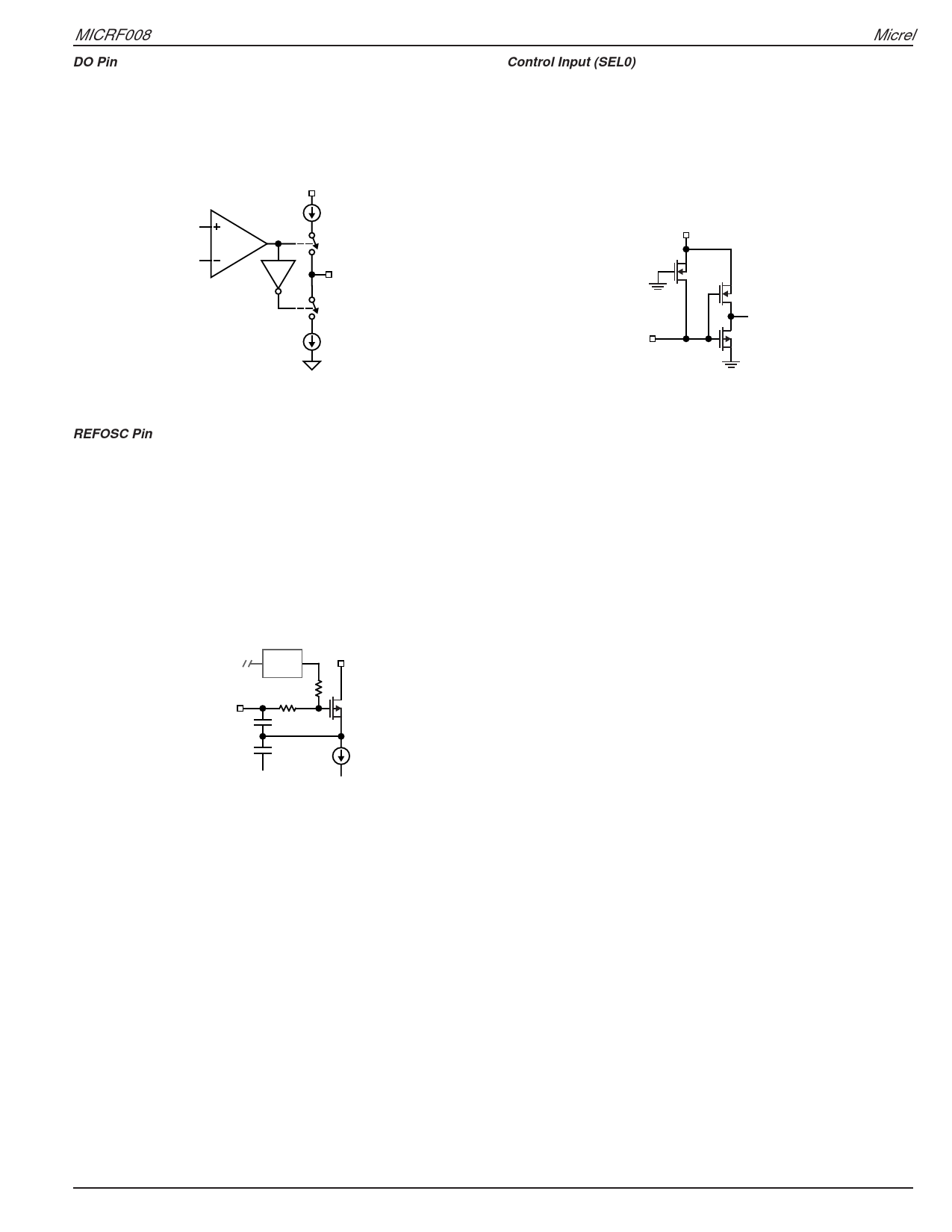
DO Pin
The output stage for the Data Comparator (DO pin) is
shown in Figure 4. The output is a 10ÎŒA push-10ÎŒA pull,
switched current stage. Such an output stage is capable
of driving CMOS-type loads.
August 2008
7
M9999-080108
Share Link: 