HV9906 Ver la hoja de datos (PDF) - Supertex Inc
Número de pieza
componentes Descripción
Fabricante
HV9906 Datasheet PDF : 10 Pages
| |||
HV9906
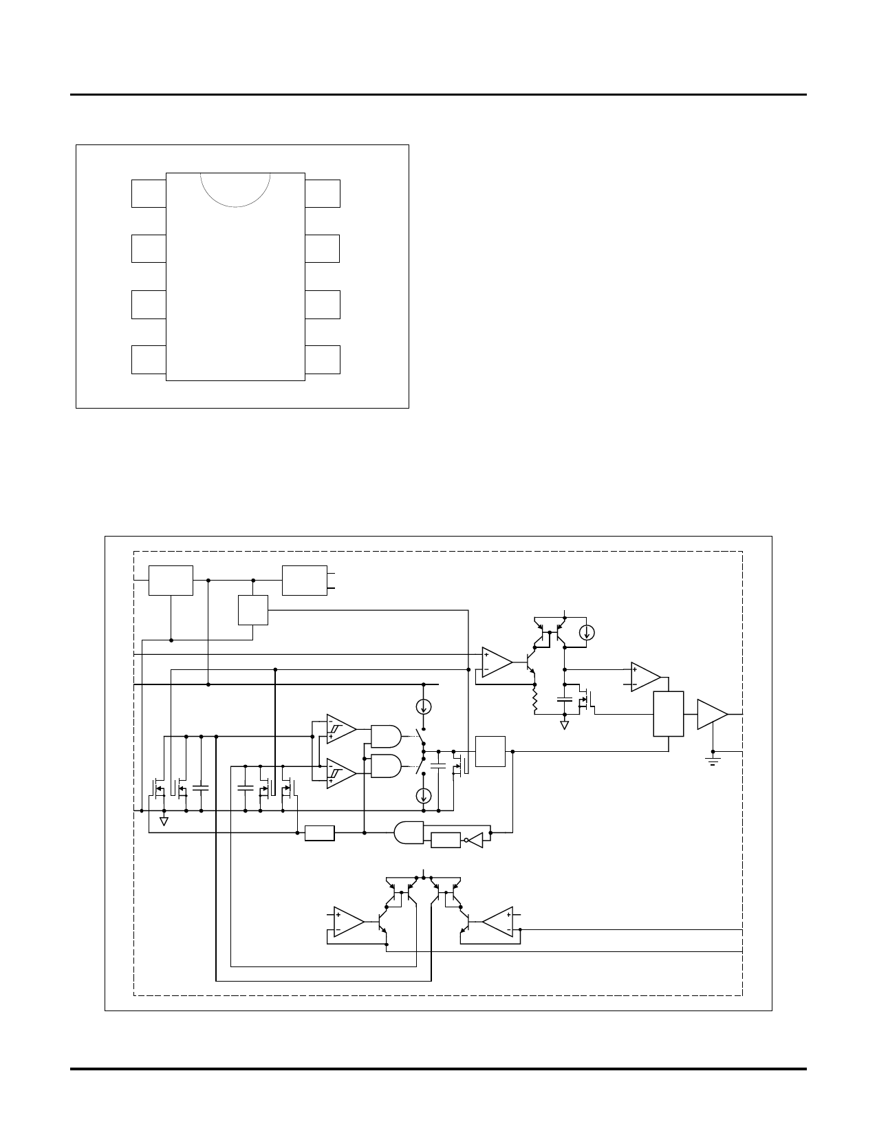
Pinout
Pin Description
+Vin 1
Von 2
Vdd 3
HV9906
8 GATE
7 PGND
6 NS
+VIN – This pin is the input to the internal linear regulator.
VON –The voltage applied to this pin by a resistor voltage divider
from +VIN controls the on time (pulse width) of the gate output.
VDD – This pin is the output of the internal linear regulator and the
supply pin for the internal circuits. It must be bypassed with a low
ESR capacitor to provide a low impedance path for the gate drive
and be capable of storing sufficient energy so that the voltage does
not decay below the UVLO threshold during the time when the
input voltage is below the minimum required by the regulator.
AGND – This pin is the common connection for analog circuits.
AGND 4
5 PS
GATE – This pin is the output for driving the gate of an external N-
channel MOSFET.
PGND – This is the common connection for the GATE drive circuit.
NS – This pin is the negative terminal of the differential sense
feedback circuit.
PS – This pin is the positive terminal of the differential sense
feedback circuit.
__________________________________________________________________________________________________________________
Functional Block Diagram
+Vin
High Voltage
Regulator
Von
Vdd
AGND
Bandgap
1V
Reference Vref
UVLO
Vdd
and
POR
Vdd
C
VCO
C
Reset Pulse
Delay Sample Pulse
Delay
Vdd
1V
1V
Vref
R
_
Q Q Driver
GATE
S
PGND
NS
PS
3
07/23/02
Supertex, Inc. 1235 Bordeaux Drive, Sunnyvale, CA 94089 TEL: (408) 744-0100 FAX: (408) 222-4895 www.supertex.com
Share Link: 