MIC5203 Ver la hoja de datos (PDF) - Micrel
Número de pieza
componentes Descripción
Fabricante
MIC5203 Datasheet PDF : 10 Pages
| |||
Micrel, Inc.
MIC5203
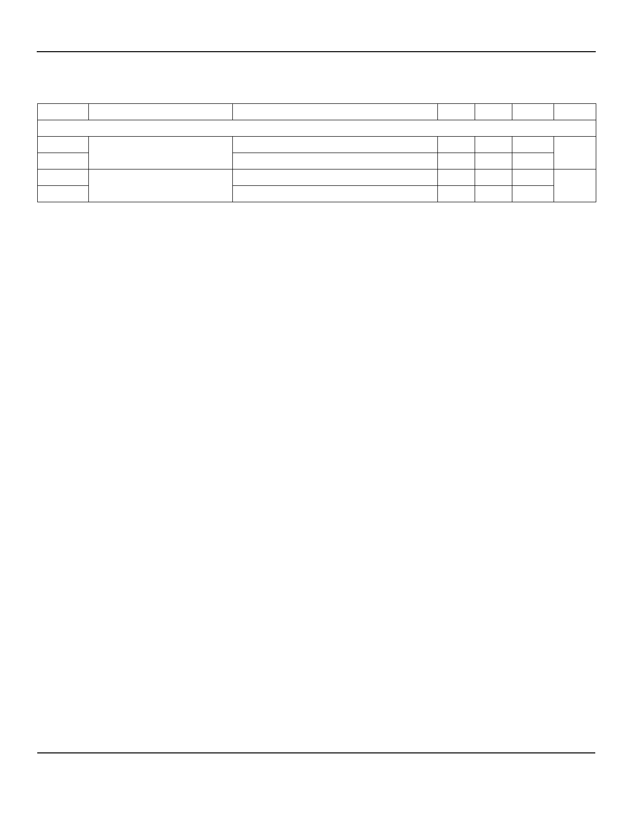
Electrical Characteristics (continued)
VIN = VOUT + 1V; IL = 1mA; CL = 0.47μF; VEN ≥ 2.0V; TJ = 25°C, bold values indicate –40°C≤ TJ ≤ +125°C, unless noted.
Symbol Parameter
Condition
Min Typ Max Units
Enable Input
VIL
Logic low (off)
Enable input voltage level
VIH
Logic high (on)
0.6
V
2.0
IIL
Enable input current
IIH
VIL ≤ 0.6V
VIH ≥ 2.0V
0.01
1
μA
15
50
Notes:
1. Exceeding the absolute maximum rating may damage the device.
2. The device is not guaranteed to function outside its operating rating.
3. The maximum allowable power dissipation at any TA (ambient temperature) is PD(MAX) = (TJ(MAX) – TA) ÷ θJA. Exceeding the maximum allowable power
dissipation will result in excessive die temperature, and the regulator will go into thermal shutdown. The θJA is 250°C/W for the SOT-143 and 220°C/W
for the SOT-23-5 mounted on a printed circuit board.
4. Output voltage temperature coefficient is defined as the worst-case voltage change divided by the total temperature range.
5. Regulation is measured at constant junction temperature using low duty cycle pulse testing. Parts are tested for load regulation in the load range from
0.1mA to 150mA. Changes in output voltage due to heating effects are covered by the thermal regulation specification.
6. Dropout voltage is defined as the input-to-output differential at which the output voltage drops 2% below its nominal value measured at 1V differential.
7. Ground pin current is the regulator quiescent current plus pass transistor base current. The total current drawn from the supply is the sum of the load
current plus the ground pin current.
8. Thermal regulation is defined as the change in output voltage at a time “t” after a change in power dissipation is applied, excluding load or line
regulation effects. Specifications are for a 150mA load pulse at VIN = 16V for t = 10ms.
November 2009
5
M9999-111909
Share Link: 