MGCT04 Ver la hoja de datos (PDF) - Zarlink Semiconductor Inc
Número de pieza
componentes Descripción
Fabricante
MGCT04 Datasheet PDF : 12 Pages
| |||
MGCT04 Preliminary Information
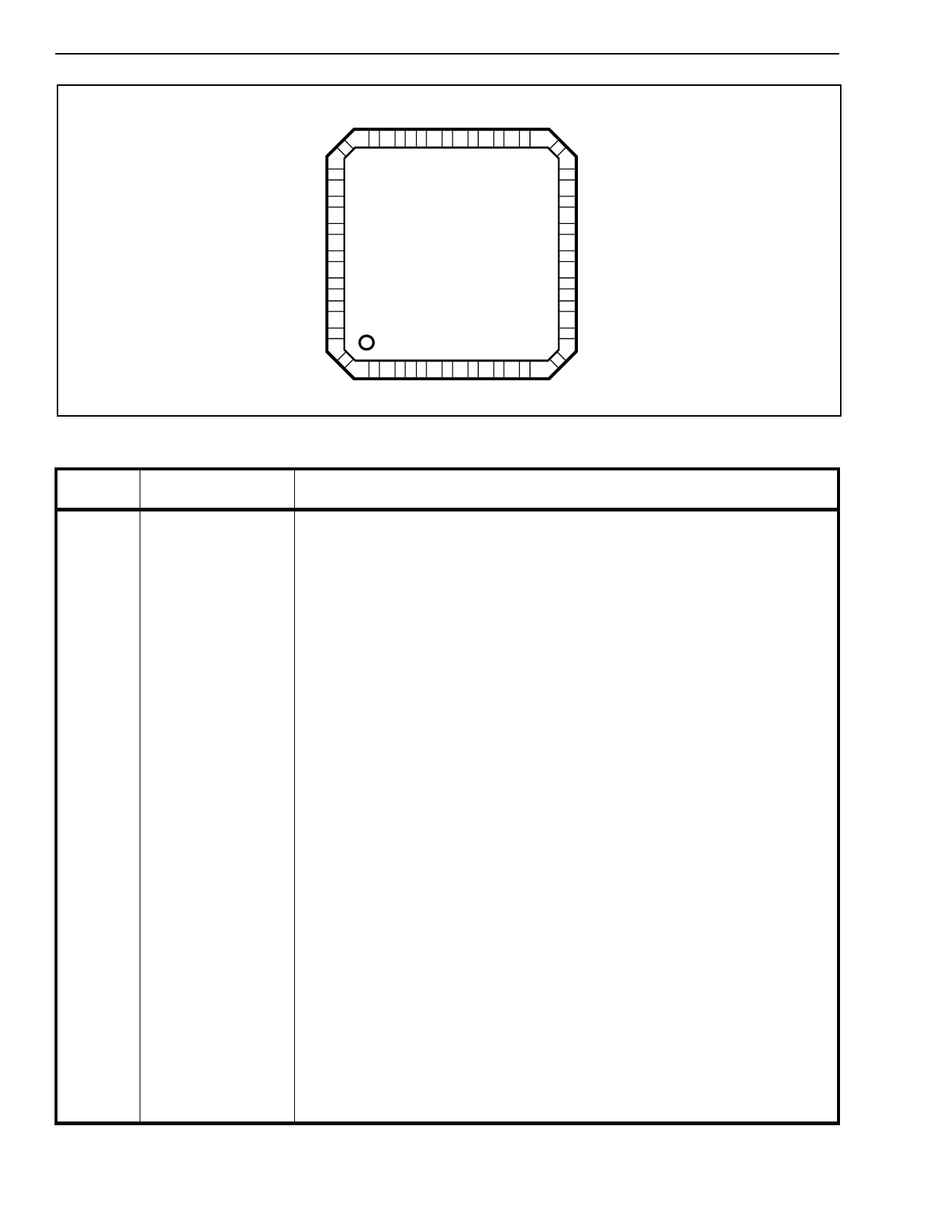
21
22
15
14
28
1
8 Note:
Corner Pads are connected
to ground
7
Figure 2 - Pin Connections - top view
Pin
Signal Name
Function
1
RF DEG2
Connection to external inductor to control gain of power amplifiers
2
RF 900B
Inverse output from 900MHz differential output driver
3
RF 900
Output from 900MHz differential output driver
4
RF GND
Ground to RF circuits
5
CP0
Control pin 0. See tables 2 & 3 for function
6
VCO GND
Ground for VHF oscillator
7
DIV OUT
Output from VHF oscillator divided by 8
8
CP2
Control pin 2. See tables 2 & 3 for function
9
VHF OSC IN
Input from external VHF oscillator
10
VHF OSC BIAS
Switched bias voltage for external VHF oscillator
11
VCO VCC
12
GND
Positive supply to VHF oscillator
Ground
13
Q IN
Q +input
14
Q INB
Q -input
15
I IN
I +input
16
I INB
I -input
17
V CC
18
UHF VCC
19
LO 2GHZ
Positive supply
Positive supply to UHF LO input buffers
2GHz local oscillator input
20
GND UHF
Ground to UHF oscillator input buffers
21
LO 1GHZ
1GHz local oscillator input
22
AGC
Control voltage for IF and RF variable gain amplifiers
23
CP1
Control pin 1. See tables 2 & 3 for function
24
RF VCC
25
RF GND
Positive supply to RF circuits
Ground to RF circuits
26
RF 1900B
Inverse output from 1900MHz differential output driver
27
RF 1900
Output from 1900MHz differential output driver
28
RF DEG1
Connection to external inductor to control gain of power amplifiers
Table 1 - Pin Assignments
2
Share Link: 