MEJ02C2016_M5M5J167KT Ver la hoja de datos (PDF) - Hitachi -> Renesas Electronics
Número de pieza
componentes Descripción
Fabricante
MEJ02C2016_M5M5J167KT
Hitachi -> Renesas Electronics

MEJ02C2016_M5M5J167KT Datasheet PDF : 11 Pages
| |||
Jan.10,2003 Ver. 2.1
M5M5J167KT - 70HI
MITSUBISHI LSIs
16777216-BIT (1048576-WORD BY 16-BIT / 2097152-WORD BY 8-BIT) CMOS STATIC RAM
DESCRIPTION
The M5M5J167KT is a f amily of low v oltage 16Mbit static RAMs
organized as 1048576-words by 16-bit / 2097152-words by 8-bit,
f abricated by Mitsubishi's high-perf ormance 0.18µm CMOS
technology .
The M5M5J167KT is suitable f or memory applications where a
simple interf acing , battery operating and battery backup are
the important design objectiv es.
The M5M5J167KT is made by stacked-micro-package technology
and two chips of 8Mbits SRAMs are assembled in one package.
By using this package technology , small package size can be
achiev ed f or highdensity SRAM.
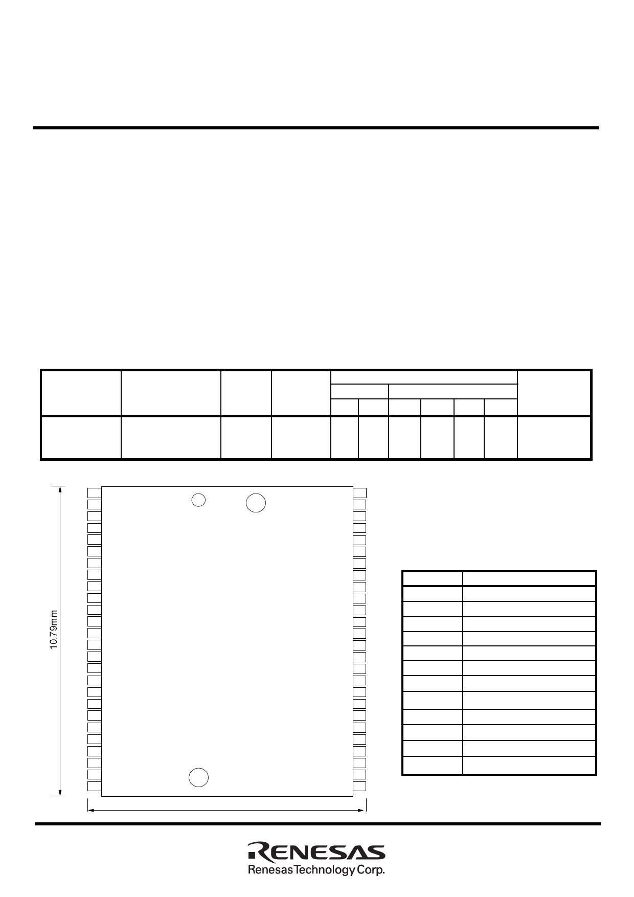
The M5M5J167KT is packaged in a 52pin-µTSOP with the outline
of 10.79mm x 10.49mm, and pin pitch of 0.40mm. It giv es the
best solution f or a compaction of m ounting area as well as
f lexibility of wiring pattern of printed circuit boards.
The operating temperature range is -40 ~ +85°C
FEATURES
- Single 2.7~3.6V power supply
- Small stand-by current: 0.2µA (2.0V, ty p.)
- No clocks, No ref resh
- Data retention supply v oltage =2.0~3.6V
- All inputs and outputs are TTL compatible.
- Easy memory expansion by S1#, S2, BC1# and BC2#
- Common Data I/O
- Three-state outputs: OR-tie capability
- OE prev ents data contention in the I/O bus
- By te f unction (x8 mode) av ailable by By te# & A-1.
- Process technology : 0.18µm CMOS
- Package: 52pin 10.79mm x 10.49mm µTSOP
[0.4mm pin pitch]
Operating
temperature
-40 ~ +85°C
Part name
Stand-by c urrent
Power Access time * Ty pical
Ratings (max.)
Supply
max. 25ºC 40ºC 25ºC 40ºC 70ºC 85ºC
M5M5J167KT -70HI 2.7 ~ 3.6V 70ns
2.0 2.4 10 16 40 80
Active
current
Icc1
(3.3V, Ty p.)
30mA
(10MHz)
5mA
(1MHz)
PIN CONFIGURATION
A15 1
A14 2
A13 3
A12 4
A11 5
A10 6
A9 7
A8 8
A19 9
S1# 10
W# 11
NC 12
NC 13
VCC 14
S2 15
NC 16
NC 17
A18 18
A17 19
A7 20
A6 21
A5 22
A4 23
A3 24
A2 25
A1 26
10.49mm
* Typical parameter indicates the value for the center
of distribution, and not 100% tested.
52 A16
51 BYTE#
50 BC2#
49 GND
48 BC1#
47 DQ16/A-1
46 DQ8
45 DQ15
44 DQ7
43 DQ14
Pin
Function
A0 ~ A18 Address input
42 DQ6
A19 Address input
41 DQ13 DQ1 ~ DQ16 Data input / output
40 DQ5
39 NC
38 DQ12
S1#
Chip select input 1
S2
Chip select input 2
37 DQ4
W#
Write control input
36 DQ11
35 DQ3
34 DQ10
33 DQ2
OE#
BC1#
BC2#
Output enable input
Lower By te (DQ1 ~ 8)
Upper By te (DQ9 ~ 16)
32 DQ9
31 DQ1
30 OE#
BYTE#
Vcc
By te (x8 mode) enable input
Power supply
29 GND
28 NC
GND Ground supply
27 A0 Outline: 52PTG-A
N C : No Connection
1
Share Link: