MCP621 Ver la hoja de datos (PDF) - Microchip Technology
Número de pieza
componentes Descripción
Fabricante
MCP621 Datasheet PDF : 44 Pages
| |||
MCP621/2/5
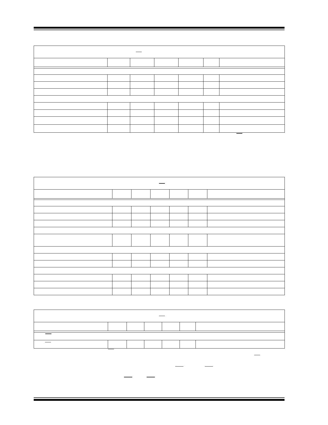
DC ELECTRICAL SPECIFICATIONS (CONTINUED)
Electrical Characteristics: Unless otherwise indicated, TA = +25°C, VDD = +2.5V to +5.5V, VSS = GND, VCM = VDD/3,
VOUT ≈ VDD/2, VL = VDD/2, RL = 2 kΩ to VL and CAL/CS = VSS (refer to Figure 1-2).
Parameters
Sym
Min
Typ
Max Units
Conditions
Calibration Input
Calibration Input Voltage Range
Internal Calibration Voltage
Input Impedance
Power Supply
VCALRNG
VCAL
ZCAL
VSS + 0.1
0.323VDD
—
—
0.333VDD
100 || 5
VDD – 1.4
0.343VDD
—
mV VCAL pin externally driven
VCAL pin open
kΩ||pF
Supply Voltage
Quiescent Current per Amplifier
POR Input Threshold, Low
VDD
IQ
VPRL
2.5
1.2
1.15
—
2.5
1.40
5.5
V
3.6
mA IO = 0
—
V
POR Input Threshold, High
VPRH
—
1.40
1.65
V
Note 1:
2:
3:
4:
Describes the offset (under the specified conditions) right after power up, or just after the CAL/CS pin is toggled. Thus,
1/f noise effects (an apparent wander in VOS; see Figure 2-35) are not included.
Increment between adjacent VOS trim points; Figure 2-3 shows how this affects the VOS repeatability.
See Figure 2-6 and Figure 2-7 for temperature effects.
The ISC specifications are for design guidance only; they are not tested.
AC ELECTRICAL SPECIFICATIONS
Electrical Characteristics: Unless otherwise indicated, TA = +25°C, VDD = +2.5V to +5.5V, VSS = GND, VCM = VDD/2,
VOUT ≈ VDD/2, VL = VDD/2, RL = 2 kΩ to VL, CL = 50 pF and CAL/CS = VSS (refer to Figure 1-2).
Parameters
Sym Min Typ Max Units
Conditions
AC Response
Gain Bandwidth Product
GBWP —
20
—
MHz
Phase Margin
PM
—
60
—
° G = +1
Open-Loop Output Impedance
AC Distortion
ROUT
—
15
—
Ω
Total Harmonic Distortion plus Noise THD+N — 0.0018 —
Step Response
% G = +1, VOUT = 2VP-P, f = 1 kHz,
VDD = 5.5V, BW = 80 kHz
Rise Time, 10% to 90%
Slew Rate
tr
—
13
—
ns G = +1, VOUT = 100 mVP-P
SR
—
10
—
V/µs G = +1
Noise
Input Noise Voltage
Input Noise Voltage Density
Input Noise Current Density
Eni
—
20
—
µVP-P f = 0.1 Hz to 10 Hz
eni
—
13
— nV/√Hz f = 1 MHz
ini
4
— fA/√Hz f = 1 kHz
DIGITAL ELECTRICAL SPECIFICATIONS
Electrical Characteristics: Unless otherwise indicated, TA = +25°C, VDD = +2.5V to +5.5V, VSS = GND, VCM = VDD/2,
VOUT ≈ VDD/2, VL = VDD/2, RL = 2 kΩ to VL, CL = 50 pF and CAL/CS = VSS (refer to Figure 1-1 and Figure 1-2).
Parameters
Sym Min Typ Max Units
Conditions
CAL/CS Low Specifications
CAL/CS Logic Threshold, Low
VIL
VSS
— 0.2VDD V
Note 1: The MCP622 has its CAL/CS input internally pulled down to VSS (0V).
2: This time ensures that the internal logic recognizes the edge. However, for the rising edge case, if CAL/CS is raised
before the calibration is complete, the calibration will be aborted and the part will return to low power mode.
3: For the MCP625 dual, there is an additional constraint. CALA/CSA and CALB/CSB can be toggled simultaneously
(within a time much smaller than tCSU) to make both op amps perform the same function simultaneously. If they are
toggled independently, then CALA/CSA (CALB/CSB) cannot be allowed to toggle while op amp B (op amp A) is in
calibration mode; allow more than the maximum tCON time (8 ms) before the other side is toggled.
DS22188A-page 4
© 2009 Microchip Technology Inc.
Share Link: 