MCP6231 Ver la hoja de datos (PDF) - Microchip Technology
NĂșmero de pieza
componentes DescripciĂłn
Fabricante
MCP6231 Datasheet PDF : 40 Pages
| |||
MCP6231/1R/1U/2/4
AC ELECTRICAL CHARACTERISTICS
Electrical Characteristics: Unless otherwise indicated, TA = +25°C, VDD = +1.8 to 5.5V, VSS = GND, VCM = VDD/2,
VOUT â VDD/2, RL = 100 kΩ to VDD/2 and CL = 60 pF.
Parameters
Sym
Min
Typ Max
Units
Conditions
AC Response
Gain Bandwidth Product
GBWP â
300
â
kHz
Phase Margin
PM
â
65
â
° G = +1 V/V
Slew Rate
SR
â
0.15
â
V/”s
Noise
Input Noise Voltage
Input Noise Voltage Density
Input Noise Current Density
Eni
â
6.0
â
”VP-P f = 0.1 Hz to 10 Hz
eni
â
52
â
nV/âHz f = 1 kHz
ini
â
0.6
â
fA/âHz f = 1 kHz
TEMPERATURE CHARACTERISTICS
Electrical Characteristics: Unless otherwise indicated, VDD = +1.8V to +5.5V and VSS = GND.
Parameters
Sym
Min
Typ
Max Units
Conditions
Temperature Ranges
Extended Temperature Range
Operating Temperature Range
Storage Temperature Range
Thermal Package Resistances
TA
-40
â
+125
°C
TA
-40
â
+125
°C Note
TA
-65
â
+150
°C
Thermal Resistance, 5L-SC70
ΞJA
â
331
â
°C/W
Thermal Resistance, 5L-SOT-23
ΞJA
â
256
â
°C/W
Thermal Resistance, 8L-DFN
ΞJA
â
84.5
â
°C/W
Thermal Resistance, 8L-MSOP
ΞJA
â
206
â
°C/W
Thermal Resistance, 8L-TDFN
ΞJA
â
41
â
°C/W
Thermal Resistance, 8L-PDIP
ΞJA
â
85
â
°C/W
Thermal Resistance, 8L-SOIC
ΞJA
â
163
â
°C/W
Thermal Resistance, 14L-PDIP
ΞJA
â
70
â
°C/W
Thermal Resistance, 14L-SOIC
ΞJA
â
120
â
°C/W
Thermal Resistance, 14L-TSSOP
ΞJA
â
100
â
°C/W
Note: The internal Junction Temperature (TJ) must not exceed the Absolute Maximum specification of +150°C.
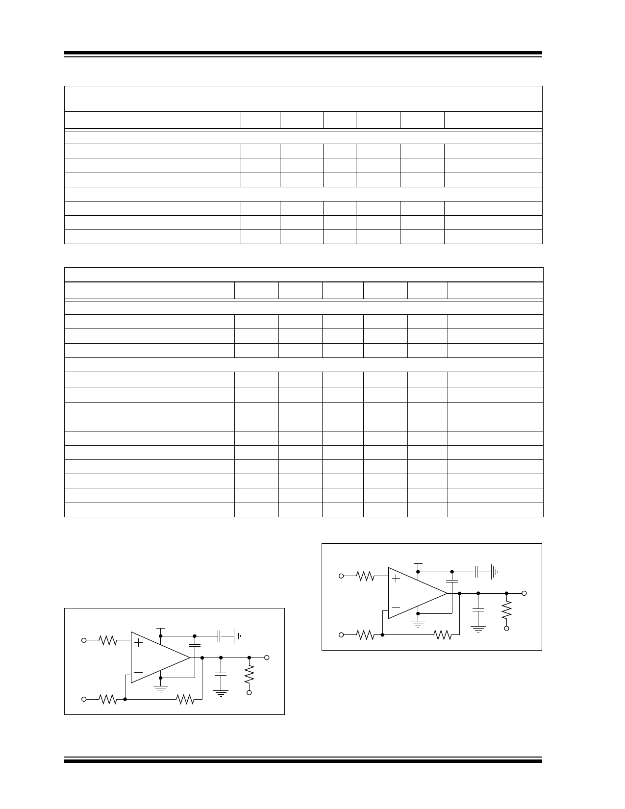
1.1 Test Circuits
The test circuits used for the DC and AC tests are
shown in Figure 1-1 and Figure 1-1. The bypass
capacitors are laid out according to the rules discussed
in Section 4.6 âPCB Surface Leakageâ.
VDD/2
RN
VDD 0.1 ”F 1 ”F
MCP623X
VOUT
VIN
RN
VDD/2 RG
VDD 0.1 ”F 1 ”F
MCP623X
RF
VOUT
CL RL
VL
VIN RG
CL RL
RF
VL
FIGURE 1-2:
AC and DC Test Circuit for
Most Inverting Gain Conditions.
FIGURE 1-1:
AC and DC Test Circuit for
Most Non-Inverting Gain Conditions.
DS21881E-page 4
© 2009 Microchip Technology Inc.
Share Link: 