MCP3903 Ver la hoja de datos (PDF) - Microchip Technology
Número de pieza
componentes Descripción
Fabricante
MCP3903 Datasheet PDF : 54 Pages
| |||
MCP3903
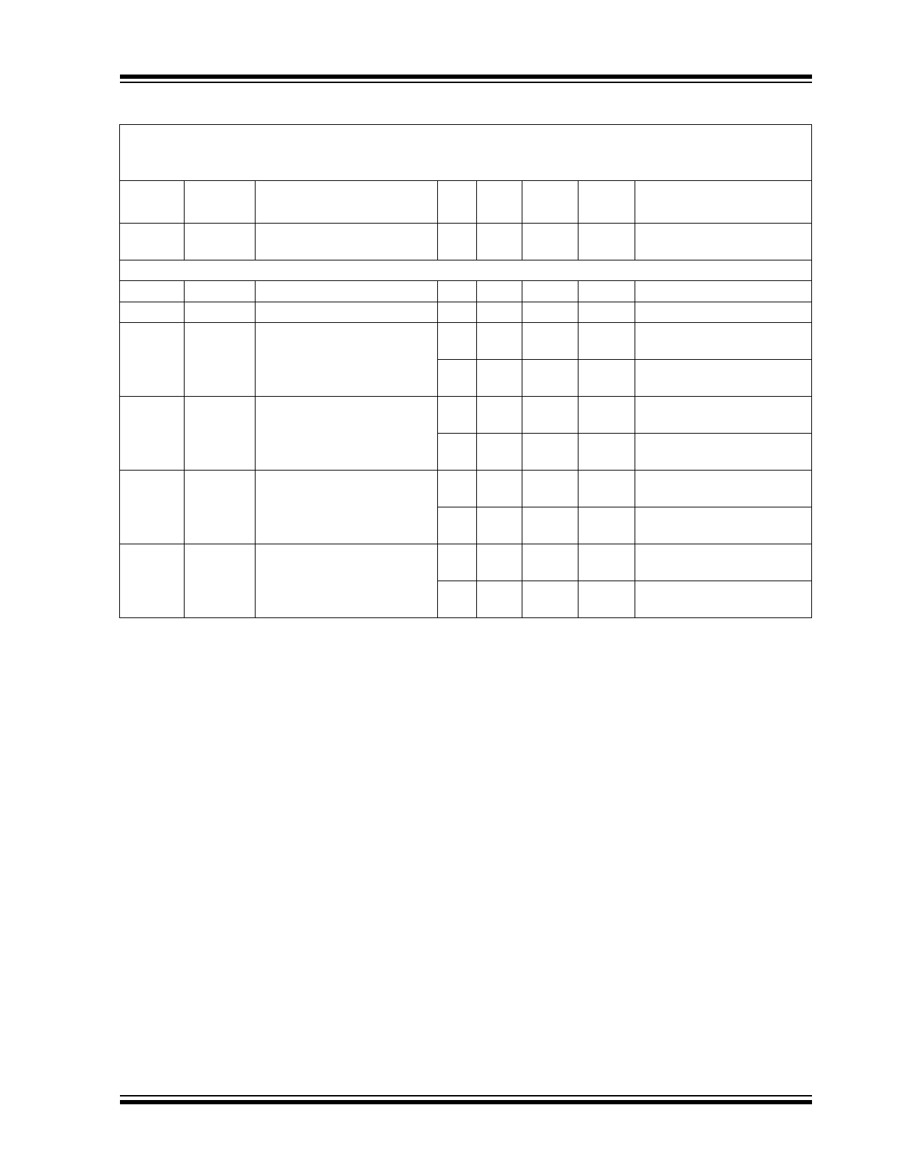
TABLE 1-1: ANALOG SPECIFICATIONS TARGET TABLE (CONTINUED)
Electrical Specifications: Unless otherwise indicated, all parameters apply at AVDD = 4.5 to 5.5V, DVDD = 2.7 to
3.6V, Internal VREF, MCLK = 4 MHz;PRESCALE = 1; OSR = 64; fS = 1 MHz; fD = 15.625 ksps; TA = -40°C to +125°C,
GAIN = 1, VIN = 1VPP = 353mVRMS @ 50/60 Hz.
Param.
Num.
Symbol
Characteristic
Min. Typ. Max. Units
Test Conditions
A028
MCLK Master Clock Frequency
Range
1 — 16.384 MHz (Note 8)
Power Specifications
P001
P002
P003
AVDD Operating Voltage, Analog
4.5 —
5.5
DVDD Operating Voltage, Digital
2.7 —
3.6
AIDD
Operating Current, Analog
(Note 4)
7.1
9
V
V
mA BOOST bits low on all chan-
nels
12.3 16.8
mA BOOST bits high on all
channels
P004
DIDD Operating Current, Digital
— 1.2 1.7
mA DVDD = 3.6V, MCLK =
4 MHz
— 2.4 3.4
mA DVDD = 3.6V, MCLK =
8.192 MHz
P005
IDDS,A Shutdown Current, Analog
——
1
μA -40°C to 85°C, AVDD pin
only, (Note 5)
——
3
μA -40°C to 125°C, AVDD pin
only, (Note 5)
P006
IDDS,D Shutdown Current, Digital
——
1
μA -40°C to 85°C, DVDD pin
only, (Note 5)
——
5
μA -40°C to 125°C, DVDD pin
only, (Note 5)
Note 1:
2:
3:
4:
5:
6:
7:
8:
This specification implies that the ADC output is valid over this entire differential range, i.e. there is no distortion or
instability across this input range. Dynamic Performance is specified at -0.5 dB below the maximum signal range,
VIN = -0.5 dBFS @ 50/60 Hz = 333 mVRMS, VREF = 2.4V.
See terminology section for definition.
This parameter is established by characterization and not 100% tested.
For these operating currents, the following configuration bit settings apply: Config Register Settings:
SHUTDOWN<5:0> = 000000, RESET<5:0> = 000000; VREFEXT = 0, CLKEXT = 0.
For these operating currents, the following configuration bit settings apply: Config Register Settings:
SHUTDOWN<5:0> = 111111, VREFEXT = 1, CLKEXT = 1.
Applies to all gains. Offset error is dependant on PGA gain setting.
Outside of this range, ADC accuracy is not specified. An extended input range of +/- 6V can be applied continuously to
the part with no risk for damage.
For proper operation and to keep ADC accuracy, AMCLK should always be in the range of 1 to 5 MHz with BOOST bits
off. With BOOST bits on, AMCLK should be in the range of 1 to 8.192 MHz. AMCLK = MCLK/PRESCALE. When using a
crystal, CLKEXT bit should be equal to ‘0’.
© 2011 Microchip Technology Inc.
DS25048B-page 5
Share Link: 