MCP1701A Ver la hoja de datos (PDF) - Microchip Technology
NГәmero de pieza
componentes DescripciГіn
Fabricante
MCP1701A Datasheet PDF : 22 Pages
| |||
MCP1701A
1.0 ELECTRICAL
CHARACTERISTICS
Absolute Maximum Ratings вҖ
Input Voltage ........................................................+12V
Output Current (Continuous)..........PD/(VIN вҖ“ VOUT)mA
Output Current (peak) ..................................... 500 mA
Output Voltage ............... (GND вҖ“ 0.3V) to (VIN + 0.3V)
Continuous Power Dissipation:
3-Pin SOT-23A ............................................ 150 mW
3-Pin SOT-89............................................... 500 mW
3-Pin TO-92 ................................................. 300 mW
вҖ Notice: Stresses above those listed under вҖңAbsolute
Maximum RatingsвҖқ may cause permanent damage to the
device. These are stress ratings only and functional operation
of the device at these or any other conditions above those
indicated in the operation sections of the specifications is not
implied. Exposure to Absolute Maximum Rating conditions for
extended periods may affect device reliability.
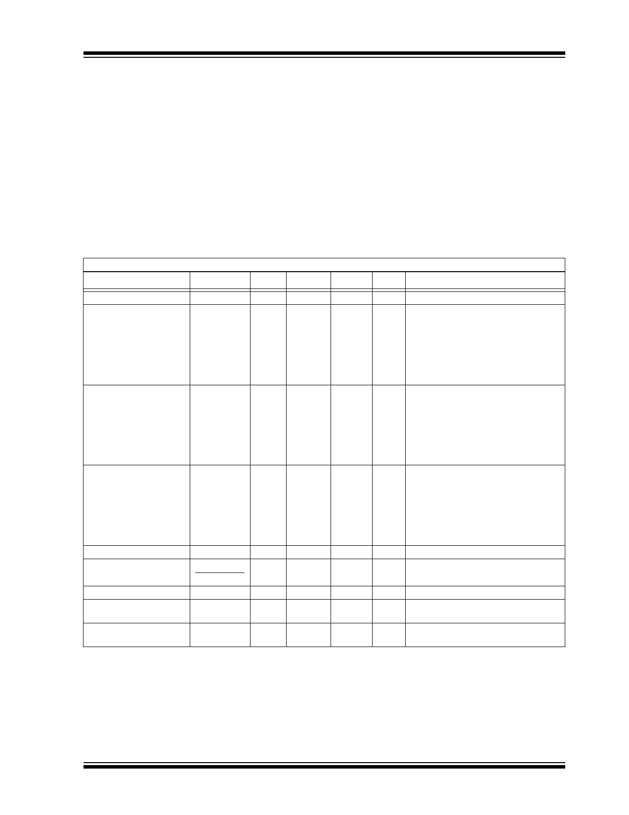
ELECTRICAL CHARACTERISTICS
Electrical Specifications: Unless otherwise specified, all limits are established for an ambient temperature of TA = +25В°C.
Parameters
Sym
Min
Typ
Max Units
Conditions
Output Voltage Regulation
VOUT
VR - 2% VRВұ0.5% VR + 2% V IOUT = 40 mA (Note 1)
Maximum Output Current
Load Regulation (Note 3)
Dropout Voltage
Input Quiescent Current
Line Regulation
Input Voltage
Temperature Coefficient of
Output Voltage
IOUTMAX
О”VOUT/ VOUT
VIN - VOUT
IQ
О”VOUTвҖў100
О”VINвҖўVOUT
VIN
TCVOUT
250
200
150
150
125
110
-1.60
-2.25
-2.72
-3.00
-3.60
-1.60
вҖ”
вҖ”
вҖ”
вҖ”
вҖ”
вҖ”
вҖ”
вҖ”
вҖ”
вҖ”
вҖ”
вҖ”
вҖ”
вҖ”
вҖ”
вҖ”
Вұ0.8
Вұ1.1
Вұ1.3
Вұ1.5
Вұ1.8
Вұ0.8
380
400
400
400
400
180
2.0
0.2
вҖ”
Вұ100
вҖ”
вҖ”
вҖ”
вҖ”
вҖ”
вҖ”
+1.60
+2.25
+2.72
+3.00
+3.60
+1.60
600
630
700
700
700
300
4.5
0.3
mA VOUT = 5.0V (VIN = VR + 1.0V)
VOUT = 4.0V
VOUT = 3.3V
VOUT = 3.0V
VOUT = 2.5V
VOUT = 1.8V
% VOUT = 5.0V, 1 mA вүӨ IOUT вүӨ 100 mA
VOUT = 4.0V, 1 mA вүӨ IOUT вүӨ 100 mA
VOUT = 3.3V, 1 mA вүӨ IOUT вүӨ 80 mA
VOUT = 3.0V, 1 mA вүӨ IOUT вүӨ 80 mA
VOUT = 2.5V, 1 mA вүӨ IOUT вүӨ 60 mA
VOUT = 1.8V, 1 mA вүӨ IOUT вүӨ 30 mA
mV IOUT = 200 mA, VR = 5.0V
IOUT = 200 mA, VR = 4.0V
IOUT = 150 mA, VR = 3.3V
IOUT = 150 mA, VR = 3.0V
IOUT = 120 mA, VR = 2.5V
IOUT = 20 mA, VR = 1.8V
ВөA VIN = VR + 1.0V
%/V IOUT = 40 mA, (VR +1) вүӨ VIN вүӨ 10.0V
10
V
вҖ”
ppm/ IOUT = 40 mA, -40В°C вүӨ TA вүӨ +85В°C
В°C (Note 2)
Output Rise Time
TR
вҖ”
200
вҖ”
Вөs 10% VR to 90% VR, VIN = 0V to VR +1V,
RL = 25О© resistive
1: VR is the nominal regulator output voltage. For example: VR = 1.8V, 2.5V, 3.3V, 4.0V, 5.0V.
The input voltage VIN = VR + 1.0V, IOUT = 40 mA.
2: TCVOUT = (VOUT-HIGH вҖ“ VOUT-LOW) *106 / (VR * О”Temperature), VOUT-HIGH = Highest voltage measured
over the temperature range. VOUT-LOW = Lowest voltage measured over the temperature range.
3: Load regulation is measured at a constant junction temperature using low duty cycle pulse testing.
В© 2007 Microchip Technology Inc.
DS21991C-page 3
Share Link: 