MC44145 Ver la hoja de datos (PDF) - Motorola => Freescale
Número de pieza
componentes Descripción
Fabricante
MC44145 Datasheet PDF : 8 Pages
| |||
MC44145
CIRCUIT DESCRIPTION
Composite Sync Separator
The composite sync separation section is comprised of
two blocks, a sync slicer and a sync amplifier, which can be
used to extract the vertical sync and composite sync
information from a video signal.
The sync separator is an adaptive slicer in which the
video signal is slightly integrated and then sliced at a ratio of
4.7 to 64 which corresponds to the sync to horizontal ratio.
Two outputs are given, one of high impedance and the other
low impedance.
A slicing sync inverting amplifier is also on–chip, allowing
one output to be used for composite sync and the other
output to be integrated and then sliced using the slicing
amplifier to extract the vertical sync information.
Clock Generation
The clock generation is made up of a wide ranging
emitter–coupled VCO followed by a switchable ÷2 to provide
a 50% duty cycle wherever required, or twice the set
frequency if an external divider is used. The clock generator
is a PLL subsection; its function is the generation of a high
frequency, line locked clock that is used for video sampling
and digitizing.
The clock output is a LSTTL–like buffer which has a limited
drive capability of two LSTTL loads.
The VCO is driven from a charge pump with selectable
current. The charge pump is driven by the phase comparator.
The phase comparator is a type IV “phase and frequency
comparator” sequential circuit.
The clock generator, the heart of a PLL, is to be closed by
means of an external divider, thus setting the synthesized
frequency. This divider could be implemented in discrete
logic or be a part of an ASIC subsystem.
Phase and Frequency Comparator
The phase comparator is fed from two input buffers, Fref
which expects a reference frequency at line rate and that is
rising edge sensitive, and NBACK which comes from the
external divider and is falling edge sensitive.
Charge pump current and output divider action are
controlled by applying suitable voltage on the appropriate
pins (respectively, NPD Gain and Div 2 EN).
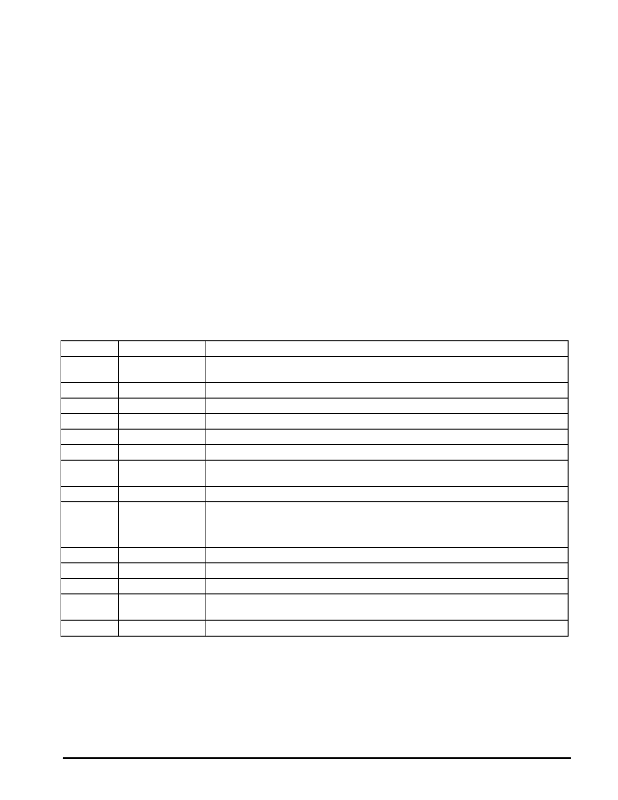
PIN FUNCTION DESCRIPTION
Pin
Function
Description
1
NPD Gain
This pin sets the gain of the phase frequency detector by changing the current of the charge pump
output (40 µA or 80 µA). Low current with this pin > 2.0 V, high current for < 0.5 V.
2
Ground
Ground connection common to the PLL and sync separator sections.
3
Sync B
High impedance sync output.
4
Sync Amp In
Sync amplifier input.
5
Sync C
Low impedance sync output.
6
VCC
7
Clock Out
Power connection to the PLL section.
VCO clock output. Capable of limited LSTTL drive. It should not be used to drive high capacitive
loads, such as long PCB traces or coaxial lines.
8
Div 2 EN
The divider is switched in with this pin > 2.0 V; switched out for < 0.5 V.
9
Fref
Reference frequency input to the phase and frequency comparator. Typically this will be a 15625
(15750) Hz signal. It is rising edge sensitive. Due to the nature of the phase and frequency
comparator, no missing pulses are tolerable on this input. In a typical setup, this signal can be
provided by the MC44011.
10
Sync Amp Out
Sync amplifier output.
11
VCC2
12
Video In
Power connection to the sync separator and amplifier.
Video signal input to the sync separator.
13
NBACK
Fed by the external clock divider. Sets the multiplication ratio of the loop in multiples of the Fref
frequency. Negative edge sensitive.
14
PLL Loop Filter
See loop filter calculations at the end of this document.
NOTE: The two VCC pins are not independent, as they are internally connected by means of the input protection diodes; they must always be both connected
to a suitable VCC line.
4
MOTOROLA ANALOG IC DEVICE DATA
Share Link: 