34710 Ver la hoja de datos (PDF) - Motorola => Freescale
Número de pieza
componentes Descripción
Fabricante
34710 Datasheet PDF : 16 Pages
| |||
Freescale Semiconductor, Inc.
SYSTEM/APPLICATION INFORMATION
INTRODUCTION
VI/O Switching Regulator
The VI/O switching regulator output voltage is determined by
the MODE digital input terminals. The 34710’s MODE[2:0]
select the output voltage (Table 1). For example, if
MODE[2:0] = 0, 0, 0, then VI/O = 5.0 V; if MODE[2:0] = Open,
Open, Open, then VI/O = 3.3 V. The MODE0 terminal controls
the output voltage of both regulators.
The topology of the regulator is a bang-bang buck regulator
operating from the internal ~200 kHz oscillator.
VCORE Linear Regulator
The VCORE linear regulator can produce a +3.3 V, 2.5 V,
1.8 V, or 1.5 V output voltage at 500 mA. The input to the
VCORE regulator is a terminal that may be connected to the VI/
O regulator output. The minimum input voltage must be
VCORE(NOM) + 0.8 V.
The MODE[2:0] terminals select the output voltage as
depicted in Table 1.
Table 1. VI/O and VCORE(NOM) Regulator
Output Voltage Selection
MODE2 MODE1 MODE0
VI /O
VCORE(NOM)
(V)
(V)
0
0
0
5.0
3.3
0
0
Open
3.3
2.5
0
Open
0
5.0
1.8
0
Open
Open
3.3
1.8
Open
0
0
5.0
2.5
Open
0
Open
3.3
2.5
Open
Open
0
5.0
1.5
Open
Open
Open
3.3
1.5
Open indicates terminal is not connected externally.
SUPERVISORY AND MISCELLANEOUS FUNCTIONS
Introduction
The supervisor circuitry provides control of the RST line, an
open drain signal, based on system operating conditions
monitored by the 34710. VI/O, VCORE, VB+, and thermal
shutdown (TSD) detectors in various parts of the chip are
monitored for error conditions. Because other devices in the
system may trigger a reset, the RST line itself is also monitored,
but the supervisor circuitry controls all reset timing, including
externally generated resets. Driving the RST line low causes the
system to be held in the reset state. VI/O, VCORE, VB+, and
thermal shutdown have both positive- and negative-going
thresholds.
The supervisor circuitry also ensures that the power supplies
sequence properly. Specifically, that VI/O is never less than
TBD V below VCORE. This means that VCORE - VI/O will be
clamped at 0.5 V, and that the VCORE regulator operation will be
suppressed during startup and shutdown to ensure that
VCORE - VI/O = TBD V.
Static Operating Specifications
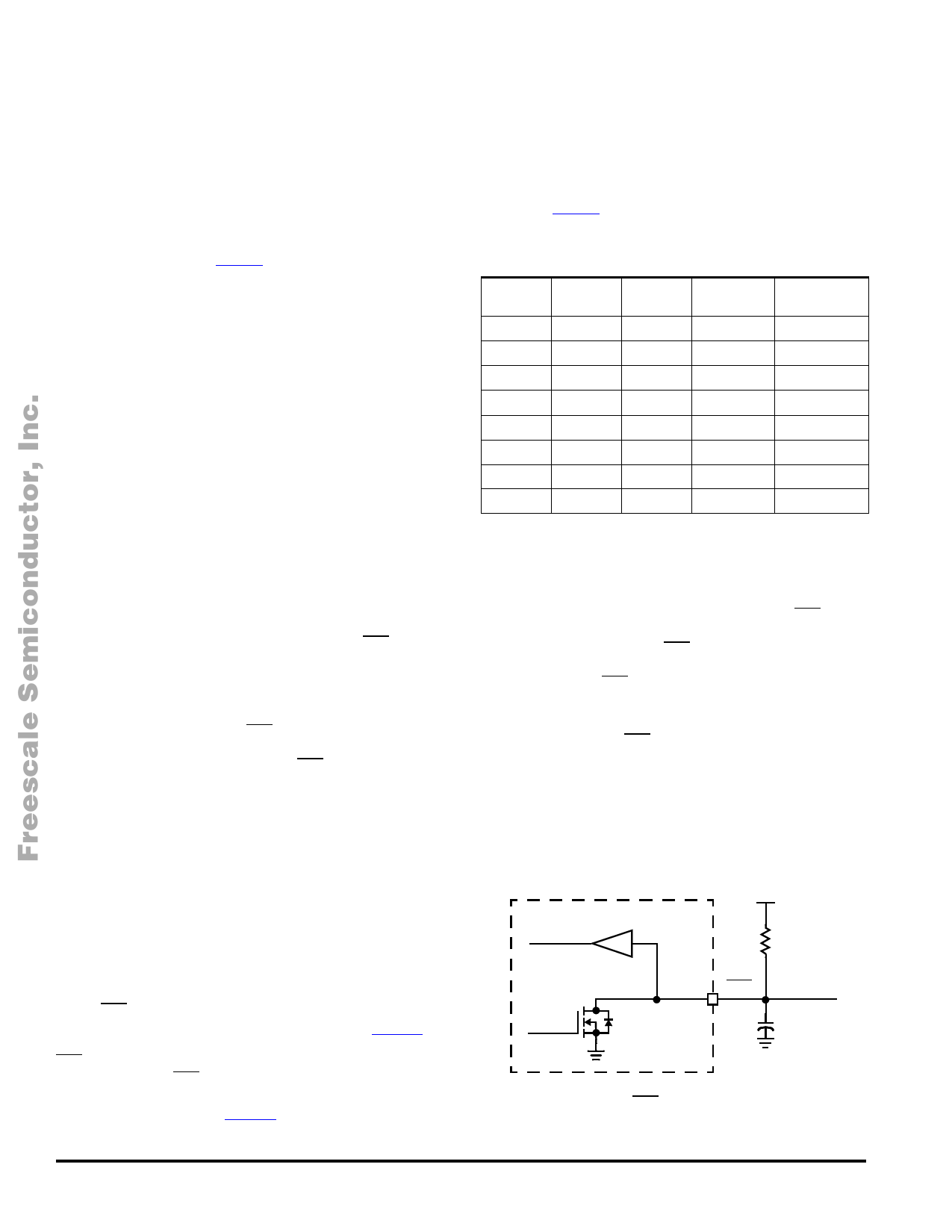
The RST output is an I/O device with an open drain output
driver with a pullup and a CMOS digital input gate (Figure 3).
This I/O structure allows wired OR connection to the MCU’s
RST I/O terminal, as well as allowing the MCU to initiate a reset
cycle by driving its RST terminal low. When responding to a
MCU request for a reset cycle, the 34710 must respond rapidly
enough to prevent a glitch. Figure 2, page 9, shows the timing
parameters for responding to an externally applied RST signal.
The rise time may be relatively slow, depending on the load
capacitance, and the internal RST input gate must operate
reliably (no oscillations during the transition) under these
conditions, i.e., the RST input can be inhibited for up to
tphsl(MAX). Error conditions must be present for a minimum
time, tfilter, before the 34710 responds to them. Once all error
conditions are cleared, RST is held low for an additional time of
tdelay. If any monitored item falls below its negative-going
threshold for tfilter, 1.0 µs to 6.0 µs, the tdelay will be restarted
when system operating conditions are met. The trigger for the
tdelay retriggerable one shot should be ([VI/O(LOW) +
VCORE(LOW) + VB+(LOW) + TJ(TSD)] & tfilter), where tfilter is the
1.0 µs to 6.0 µs delay.
To Internal
Gates
From
Internal
Reset
Circuits
VI/O
RST
RPULLUP
≥ 4.7 kΩ
(Optional)
CLOAD
(Optional)
Figure 3. RST Terminal Interface
34710
10
For More Information OMnOTTOhRiOsLAPAroNdALuOcGt,INTEGRATED CIRCUIT DEVICE DATA
Go to: www.freescale.com
Share Link: 