MC34016P Ver la hoja de datos (PDF) - Motorola => Freescale
Número de pieza
componentes Descripción
Fabricante
MC34016P Datasheet PDF : 16 Pages
| |||
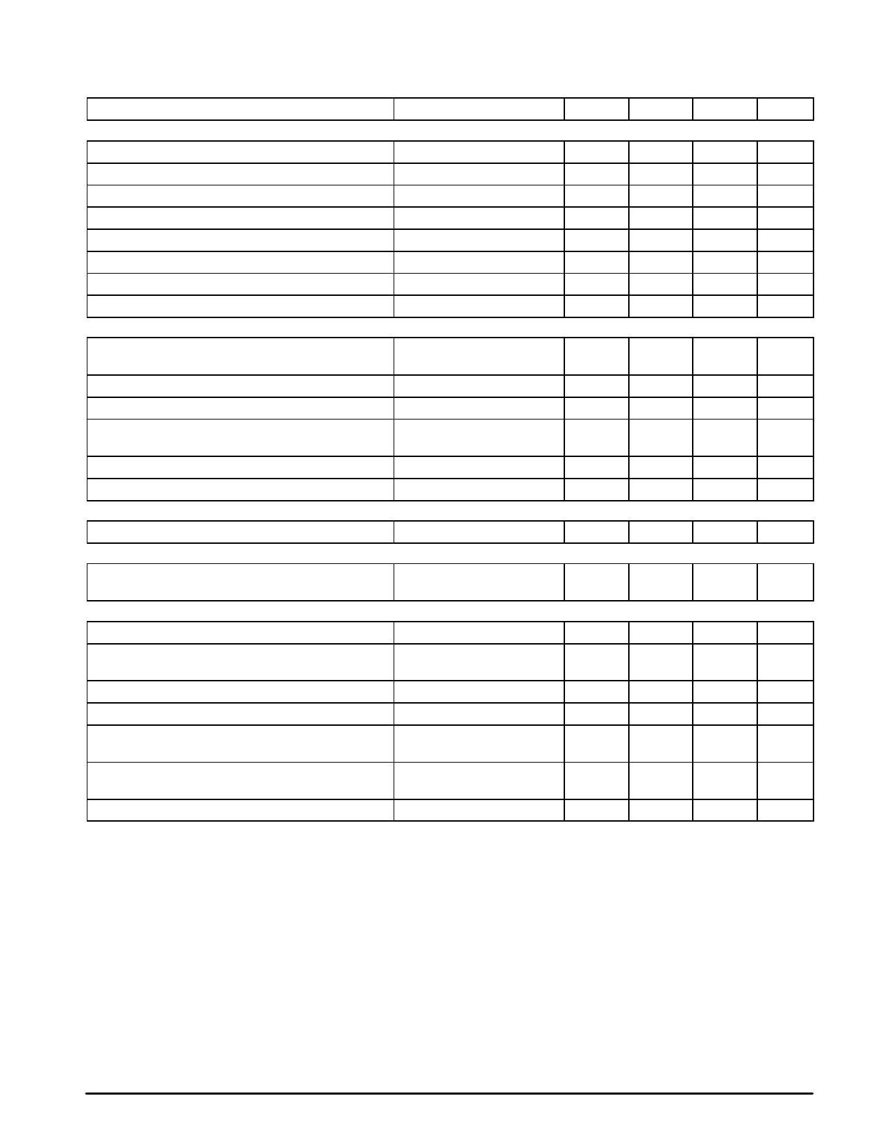
MC34016
AC ELECTRICAL CHARACTERISTICS (continued) (All parameters are specified with Bit 0 of Register 1 set to 1, the rest of the
bits in both registers set to 0, TA = 25°C, VCC = 5.0 V, Iline = 15 mA, f = 1.0 kHz, Test Circuit in Figure 9, unless otherwise noted.)
Parameter
Condition
Min
Typ
Max
Unit
RECEIVE CHANNEL
Gain Increase in 6.0 dB Mode
Bit 5, Reg. 2 = 1
5.3
6.0
6.7
dB
Gain Reduction in Mute Condition
Bit 3, Reg. 2 = 1
70
–
–
dB
Input Impedance at HYL or HYS
–
–
30
–
kΩ
Output Impedance at Rx1 or Rx2
Maximum Input Swing at HYL or HYS
–
for THD ≤ 2%
–
150
–
Ω
–
800
–
mVpp
Maximum Output Swing VRx
for THD ≤ 10%
–
3.5
–
Vpp
Total Harmonic Distortion at VRx
Vline = 3.0 dBm
–
1.0
2.0
%
Psophometrically Weighted Noise Level at VRx
200 Ω Between Tx1 and Tx2
–
80
–
µVrms
AUTOMATIC GAIN CONTROL
Gain Reduction in Transmit and Receive Channel with
Respect to Iline = 15 mA
Iline = 70 mA
5.0
6.0
7.0
dB
Highest Line Current for Maximum Gain
–
–
20
–
mA
Lowest Line Current for Minimum Gain
–
–
60
–
mA
Gain Reduction in Transmit and Receive Channel with
Respect to Iline = 35 mA
Highest Line Current for Maximum Gain
Iline = 85 mA,
Bit 1, Reg. 2 = 1
Bit 1, Reg. 2 = 1
5.0
6.0
7.0
dB
–
40
–
mA
Lowest Line Current for Minimum Gain
Bit 1, Reg. 2 = 1
–
80
–
mA
BALANCE RETURN LOSS
Balance Return Loss with Respect to 600Ω
f = 1.0 kHz
20
–
–
dB
SIDETONE
Voltage Gain from VTx to VRx
Iline = 15 mA,
Bit 0, Reg. 2 = 1
–
–
–20
dB
SERIAL BUS
Clock Frequency
–
–
–
550
kHz
BEN Rising Edge Setup Time Before First Clk Rising
See t1 in Timing Diagram
500
–
Edge
–
ns
Data Setup Time Before Clk Rising Edge
See t2 in Timing Diagram
500
–
–
ns
Data Hold Time After Clk Rising Edge
See t3 in Timing Diagram
500
–
–
ns
BEN Falling Edge Delay Time After Last Clk Rising
Edge
See t4 in Timing Diagram
1.5
–
–
µs
BEN Rising Edge Delay Time After Last BEN Falling
See t5 in Timing Diagram
6.0
–
Edge
–
µs
Power Supply Reset Voltage VCC
–
–
2.5
–
V
4
MOTOROLA ANALOG IC DEVICE DATA
Share Link: 