MC33260P Ver la hoja de datos (PDF) - ON Semiconductor
Número de pieza
componentes Descripción
Fabricante
MC33260P
ON Semiconductor

MC33260P Datasheet PDF : 22 Pages
| |||
MC33260
Pin Numbers are Relevant to the PDIP−8 Version
This equation shows that the maximum on−time is inversely
proportional to the squared output voltage. This property is
used for follower boost operation (refer to Follower Boost
section).
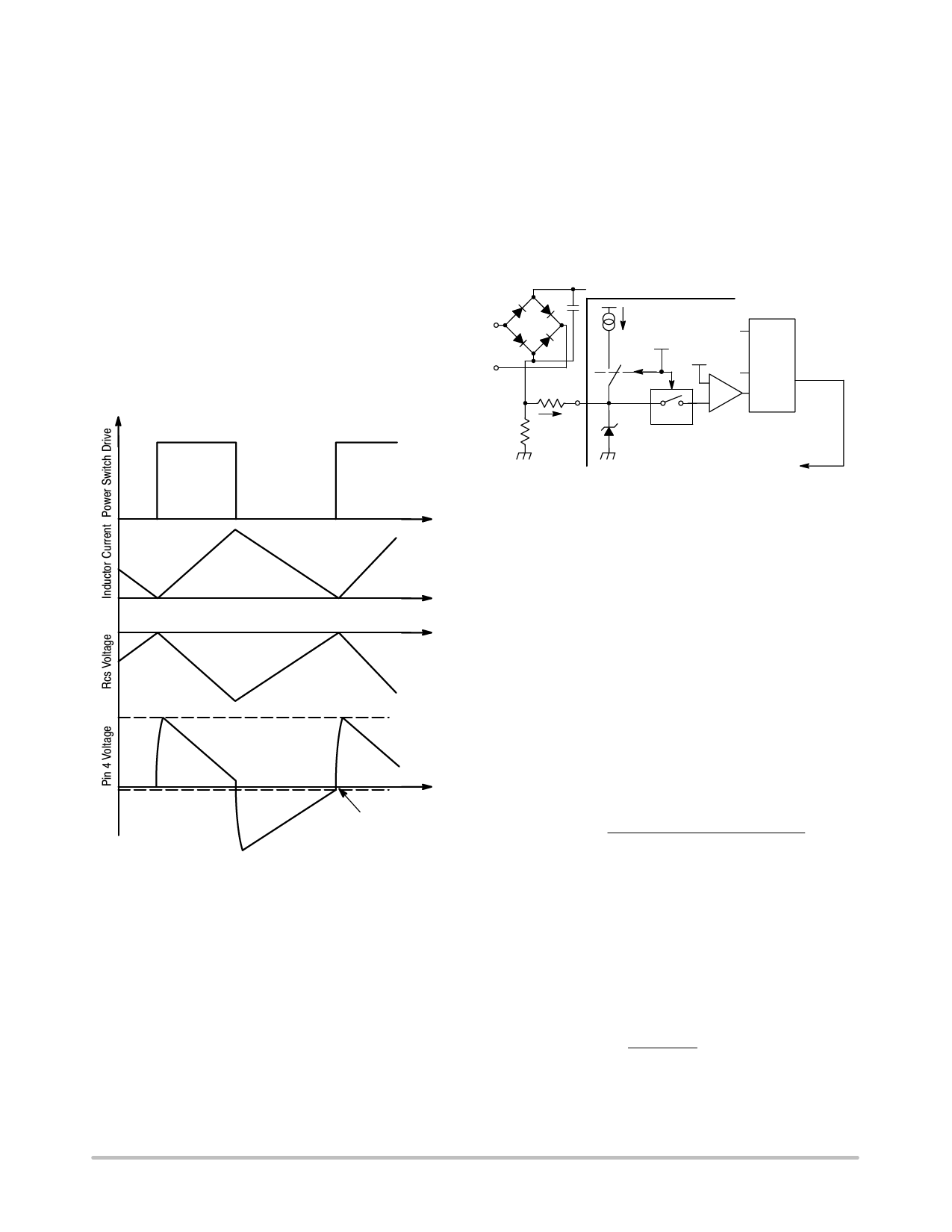
CURRENT SENSE BLOCK
The inductor current is converted into a voltage by
inserting a ground referenced resistor (Rcs) in series with the
input diodes bridge (and the input filtering capacitor).
Therefore a negative voltage proportional to the inductor
current is built:
Vcs + −ǒRcs ILǓ
where:
IL is the inductor current,
Rcs is the current sense resistor,
Vcs is the measured Rcs voltage.
Zero Current Detection
The Zero Current Detection function guarantees that the
MOSFET cannot turn on as long as the inductor current
hasn’t reached zero (discontinuous mode).
The Pin 4 voltage is simply compared to the (−60 mV)
threshold so that as long as Vcs is lower than this threshold,
the circuit gate drive signal is kept in low state.
Consequently, no power MOSFET turn on is possible until
the inductor current is measured as smaller than (60 mV/Rcs)
that is, the inductor current nearly equals zero.
D1...D4
1
ROCP
4
Rcs VOCP
Iocp (205 mA)
Output_Ctrl
−60 mV
0
+
−
LEB
S
PWM
Latch
R
Output_Ctrl
Q
R
Time
VOCP
−60 mV
Zero Current Detection
VOCP = ROCP IOCP
An overcurrent is detected if Vpin4 crosses the threshold (−60 mV)
during the Power Switch on state
Figure 27. Current Sensing
The negative signal Vcs is applied to the current sense
through a resistor ROCP. The pin is internally protected by a
negative clamp (−0.7 V) that prevents substrate injection.
As long as the Pin 4 voltage is lower than (−60 mV), the
Current Sense comparator resets the PWM latch to force the
gate drive signal low state. In that condition, the power
MOSFET cannot be on.
During the on−time, the Pin 4 information is used for the
overcurrent limitation while it serves the zero current
detection during the off time.
To Output Buffer
(Output_Ctrl Low <=> Gate Drive in Low State)
Figure 28. Current Sense Block
Overcurrent Protection
During the power switch conduction (i.e. when the Gate
Drive Pin voltage is high), a current source is applied to the
Pin 4. A voltage drop VOCP is then generated across the
resistor ROCP that is connected between the sense resistor
and the Current Sense Pin (refer to Figure 28). So, instead of
Vcs, the sum (Vcs + VOCP) is compared to (−60 mV) and the
maximum permissible current is the solution of the
following equation:
−ǒRcs IpkmaxǓ ) VOCP + −60 mV
where:
Ipkmax is maximum allowed current,
Rcs is the sensing resistor.
The overcurrent threshold is then:
ǒ Ipkmax + ROCP
Ǔ IOCP ) 60
Rcs
10−3
where:
ROCP is the resistor connected between the pin and the
sensing resistor (Rcs),
IOCP is the current supplied by the Current Sense Pin
when the gate drive signal is high (power switch
conduction phase). IOCP equals 205 mA typically.
Practically, the VOCP offset is high compared to 60 mV
and the precedent equation can be simplified. The maximum
current is then given by the following equation:
Ipkmax
[
ROCP(kW)
Rcs(W)
0.205 (A)
Consequently, the ROCP resistor can program the OCP level
whatever the Rcs value is. This gives a high freedom in the
choice of Rcs. In particular, the inrush resistor can be utilized.
http://onsemi.com
11
Share Link: