MC33067DWR2 Ver la hoja de datos (PDF) - ON Semiconductor
Número de pieza
componentes Descripción
Fabricante
MC33067DWR2
ON Semiconductor

MC33067DWR2 Datasheet PDF : 16 Pages
| |||
MC34067, MC33067
The minimum frequency is programmed by ROSC using
Equation 1:
1−
ƒ(min)
tPD
t(max)− 70 ns
ǒ Ǔ ROSC =
COSC ȏn
5.1
3.6
=
0.348 COSC
(eq. 1)
where tPD is the internal propagation delay.
The maximum oscillator frequency is set by the current
through resistor RVFO. The current required to discharge
COSC at the maximum oscillator frequency can be calculated
by Equation 2:
I(max) = COSC
5.1 − 3.6
1
ƒ(max)
= 1.5COSC ƒ(max)
(eq. 2)
The discharge current through ROSC must also be known
and can be calculated by Equation 3:
ǒ Ǔ 1
ƒ(min)
−
ǒ IROSC =
5.1 − 3.6
ROSC
ε
ROSCCOSC
−
1
Ǔ (eq. 3)
= 1.5 ε
ƒ(min) ROSCCOSC
ROSC
Resistor RVFO can now be calculated by Equation 4:
RVFO
=
2.5 − VEAsat
I(max) − IROSC
(eq. 4)
One−Shot Timer
The One−Shot is designed to disable both outputs
simultaneously providing a deadtime before either output is
enabled. The One−Shot capacitor (CT) is charged
concurrently with the oscillator capacitor by transistor Q1,
as shown in Figure 16. The one−shot period begins when the
oscillator comparator turns off Q1, allowing CT to
discharge. The period ends when resistor RT discharges CT
to the threshold of the One−Shot comparator. The lower
threshold of the One−Shot is 3.6 V. By choosing CT, RT can
by solved by Equation 5:
ǒ Ǔ R T
=
t OS
CT ȏn
5.1
3.6
=
t OS
0.348 CT
(eq. 5)
Errors in the threshold voltage and propagation delays
through the output drivers will affect the One−Shot period.
To guarantee accuracy, the output pulse of the control chip
is trimmed to within 5% of 250 ns with nominal values of RT
and CT.
The outputs of the Oscillator and One−Shot comparators
are OR’d together to produce the pulse tOS, which drives the
Flip−Flop and output drivers. The output pulse (tOS) is
initiated by the Oscillator and terminated by the One−Shot
comparator. With zero voltage resonant mode converters,
the oscillator discharge time should never be set less than the
one−shot period.
Error Amplifier
A fully accessible high performance Error Amplifier is
provided for feedback control of the power supply system.
The Error Amplifier is internally compensated and features
dc open loop gain greater than 70 dB, input offset voltage of
less than 10 mV and a guaranteed minimum gain−bandwidth
product of 2.5 MHz. The input common mode range extends
from 1.5 V to 5.1 V, which includes the reference voltage.
Oscillator
Control Current
3
IOSC
RVFO
6
Error Amp Output
8
Noninverting Input
Inverting Input 7
Error
Amp
3.1 V
Error Amp
Clamp
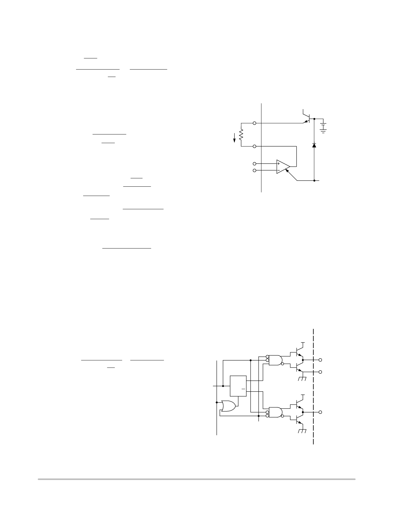
Figure 17. Error Amplifier and Clamp
When the Error Amplifier output is coupled to the IOSC
pin by RVFO, as illustrated in Figure 17, it provides the
Oscillator Control Current, IOSC. The output swing of the
Error Amplifier is restricted by a clamp circuit to improve
its transient recovery time.
Output Section
The pulse(tOS), generated by the Oscillator and One−Shot
timer is gated to dual totem−pole output drives by the
Steering Flip−Flop shown in Figure 18. Positive transitions
of tOS toggle the Flip−Flop, which causes the pulses to
alternate between Output A and Output B. The flip−flop is
reset by the undervoltage lockout circuit during startup to
guarantee that the first pulse appears at Output A.
VCC
Steering
Flip−Flop
Q
T
RQ
PWR
GND
VCC
Output A
14
Power Ground
13
Output B
12
PWR
GND
Figure 18. Steering Flip−Flop and Output Drivers
http://onsemi.com
9
Share Link: