MC1455 Ver la hoja de datos (PDF) - ON Semiconductor
Número de pieza
componentes Descripción
Fabricante
MC1455 Datasheet PDF : 11 Pages
| |||
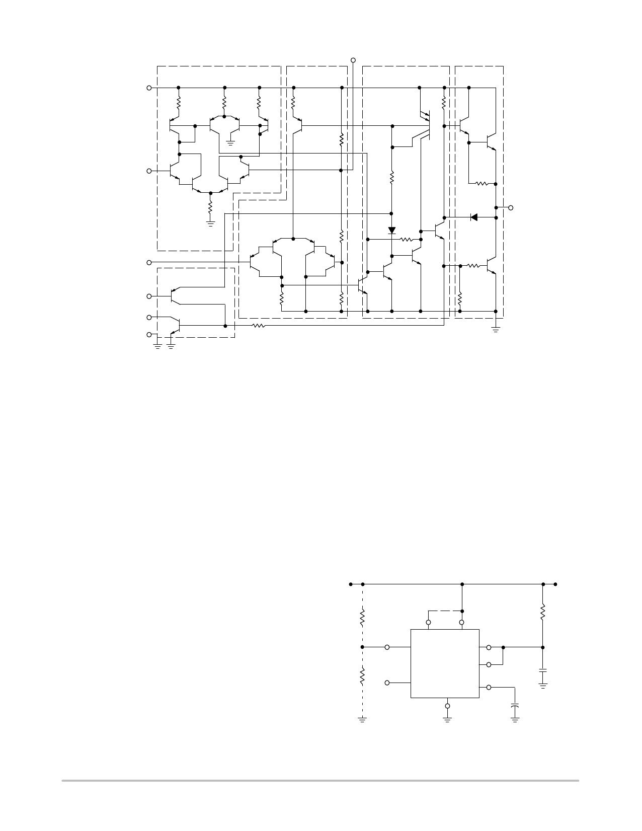
MC1455, MC1455B, NCV1455B
Control Voltage
Threshold
Comparator
Trigger
Comparator
Flip-Flop
Output
VCC
4.7 k
830
4.7 k 1.0 k
6.8 k
5.0 k
Threshold
7.0 k
Trigger
Reset
Discharge
GND
10 k
cb
5.0 k
e 4.7 k
Reset
100 k
5.0 k
Discharge
100
Figure 13. Representative Circuit Schematic
3.9 k
cb
Output
220
4.7 k
GENERAL OPERATION
The MC1455 is a monolithic timing circuit which uses an
external resistor − capacitor network as its timing element. It
can be used in both the monostable (one−shot) and astable
modes with frequency and duty cycle controlled by the
capacitor and resistor values. While the timing is dependent
upon the external passive components, the monolithic circuit
provides the starting circuit, voltage comparison and other
functions needed for a complete timing circuit. Internal to the
integrated circuit are two comparators, one for the input
signal and the other for capacitor voltage; also a flip−flop and
digital output are included. The comparator reference
voltages are always a fixed ratio of the supply voltage thus
providing output timing independent of supply voltage.
Monostable Mode
In the monostable mode, a capacitor and a single resistor
are used for the timing network. Both the threshold terminal
and the discharge transistor terminal are connected together
in this mode (refer to circuit in Figure 14). When the input
voltage to the trigger comparator falls below 1/3 VCC, the
comparator output triggers the flip−flop so that its output sets
low. This turns the capacitor discharge transistor “off” and
drives the digital output to the high state. This condition
allows the capacitor to charge at an exponential rate which is
set by the RC time constant. When the capacitor voltage
reaches 2/3 VCC, the threshold comparator resets the
flip−flop. This action discharges the timing capacitor and
returns the digital output to the low state. Once the flip−flop
has been triggered by an input signal, it cannot be retriggered
until the present timing period has been completed. The time
that the output is high is given by the equation t = 1.1 RA C.
Various combinations of R and C and their associated times
are shown in Figure 16. The trigger pulse width must be less
than the timing period.
A reset pin is provided to discharge the capacitor, thus
interrupting the timing cycle. As long as the reset pin is low,
the capacitor discharge transistor is turned “on” and prevents
the capacitor from charging. While the reset voltage is applied
the digital output will remain the same. The reset pin should
be tied to the supply voltage when not in use.
+VCC (5.0 V to 15 V)
Reset
RL
4
Output
VCC
RA
8
Discharge
7
3
RL 2
Trigger
MC1455
1
6
Threshold
5
Control
Voltage
C
0.01 mF
Figure 14. Monostable Circuit
http://onsemi.com
5
Share Link: 