MC14549B Ver la hoja de datos (PDF) - ON Semiconductor
Número de pieza
componentes Descripción
Fabricante
MC14549B Datasheet PDF : 9 Pages
| |||
MC14549B, MC14559B
OPERATING CHARACTERISTICS
Both the MC14549B and MC14559B can be operated in
either the “free run” or “strobed operation” mode for
conversion schemes with any number of bits. Reliable
cascading and/or recirculating operation can be achieved if
the End of Convert (EOC) output is used as the controlling
function, since with EOC = 0 (and with SC = 1 for
MC14549B but either 1 or 0 for MC14559B) no stable state
exists under continual clocked operation. The MC14559B
will automatically recirculate after EOC = 1 during externally
strobed operation, provided SC = 1.
All data and control inputs for these devices are triggered
into the circuit on the positive edge of the clock pulse.
Operation of the various terminals is as follows:
C = Clock — A positive−going transition of the Clock is
required for data on any input to be strobed into the circuit.
SC = Start Convert — A conversion sequence is initiated
on the positive−going transition of the SC input on
succeeding clock cycles.
D = Data in — Data on this input (usually from a
comparator in A/D applications) is also entered into the
circuit on a positive−going transition of the clock. This input
is Schmitt triggered and synchronized to allow fast response
and guaranteed quality of serial and parallel data.
MR = Master Reset (MC14549B Only) — Resets all
output to 0 on positive−going transitions of the clock. If
removed while SC = 0, the circuit will remain reset until
SC = 1. This allows easy cascading of circuits.
FF = Feed Forward (MC14559B Only) — Provides
register shortening by removing unwanted bits from a system.
For operation with less than 8 bits, tie the output following
the least significant bit of the circuit to EOC. E.g., for a 6−bit
conversion, tie Q1 to FF; the part will respond as shown in the
timing diagram less two bit times. Not that Q1 and Q0 will
still operate and must be disregarded.
For 8−bit operation, FF is tied to VSS.
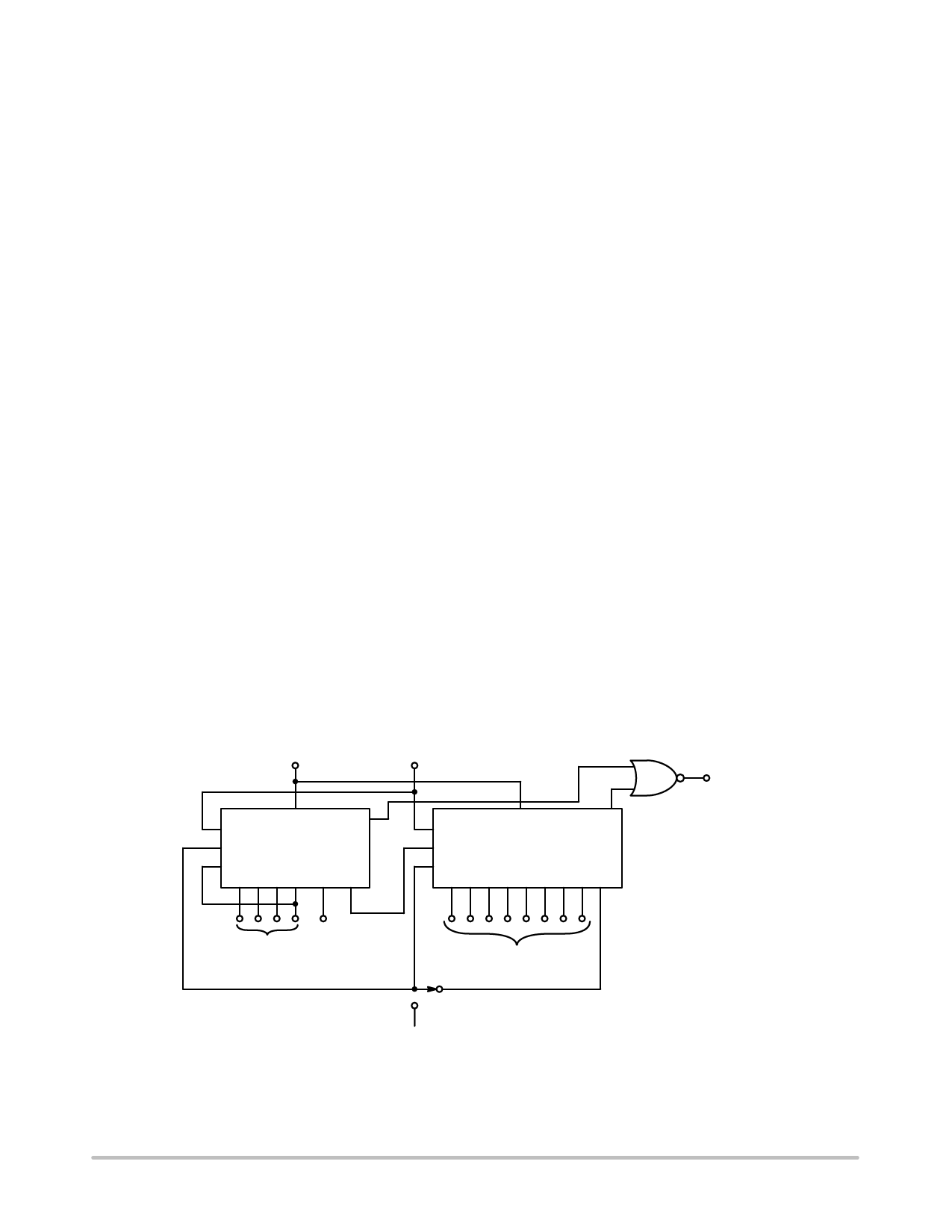
For applications with more than 8 but less than 16 bits, use
the basic connections shown in Figure 1. The FF input of the
MC14559B is used to shorten the setup. Tying FF directly to
the least significant bit used in the MC14559B allows EOC
to provide the cascading signal, and results in smooth
transition of serial information from the MC14559B to the
MC14549B. The Serial Out (Sout) inhibit structure of the
MC14559B remains inactive one cycle after EOC goes high,
while Sout of the MC14549B remains inhibited until the
second clock cycle of its operation.
Qn = Data Outputs — After a conversion is initiated the
Q’s on succeeding cycles go high and are then conditionally
reset dependent upon the state of the D input. Once
conditionally reset they remain in the proper state until the
circuit is either reset or reinitiated.
EOC = End of Convert — This output goes high on the
negative−going transition of the clock following FF = 1 (for
the MC14559B) or the conditional reset of Q0. This allows
settling of the digital circuitry prior to the End of Conversion
indication. Therefore either level or edge triggering can
indicate complete conversion.
Sout = Serial Out — Transmits conversion in serial
fashion. Serial data occurs during the clock period when the
corresponding parallel data bit is conditionally reset. Serial
Out is inhibited on the initial period of a cycle, when the
circuit is reset, and on the second cycle after EOC goes high.
This provides efficient operation when cascaded.
FROM A/D
COMPARATOR
EXTERNAL
CLOCK
1/4 MC14001
C
D
Sout
SC MC14559B
* FF
Q7 Q6 Q5 Q4 •• Q0 EOC
**
MSB
NC
TO D/A AND PARALLEL DATA
C
D
Sout
SC
MC14549B
MR
Q7 Q6 Q5 Q4 Q3 Q2 Q1 Q0 EOC
{
LSB
TO D/A AND
PARALLEL DATA
FREE RUN MODE
EXTERNAL STROBE
* FF allows EOC to activate as if in 4−stage register.
** Cascading using EOC guaranteed; no stable unfunctional state.
†Completion of conversion automatically re−initiates cycle in free run mode.
Figure 1. 12−Bit Conversion Scheme
SERIAL OUT
(CONTINUAL
UPDATE EVERY
13 CLOCK CYCLES)
http://onsemi.com
5
Share Link: 