MC14549B Ver la hoja de datos (PDF) - Motorola => Freescale
Número de pieza
componentes Descripción
Fabricante
MC14549B Datasheet PDF : 9 Pages
| |||
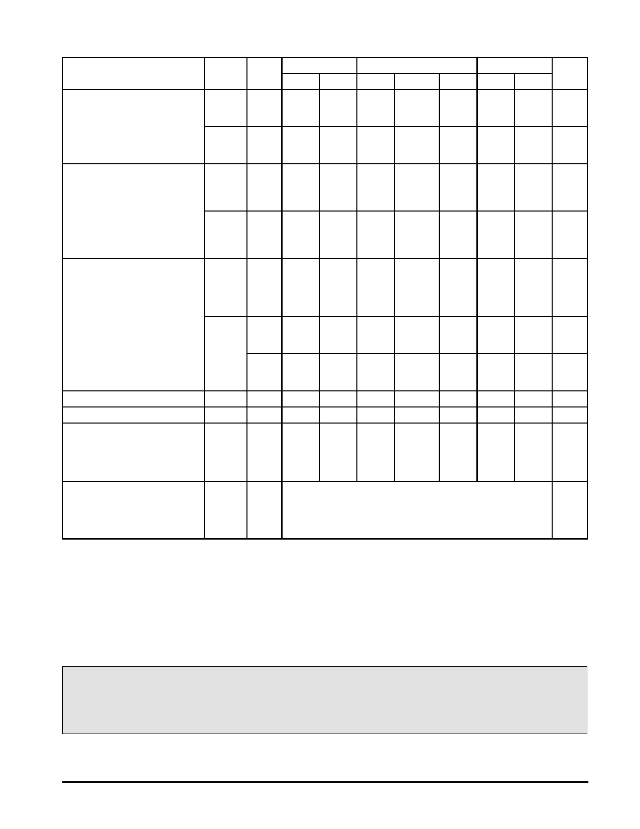
ÎÎÎÎEÎÎÎÎLEÎÎÎÎCTRÎÎÎÎICAÎÎÎÎL CÎÎÎÎHAÎÎÎÎRACÎÎÎÎTEÎÎÎÎRISÎÎÎÎTICÎÎÎÎS (VÎÎÎÎoltagÎÎÎÎesVRÎÎÎÎDefDerÎÎÎÎencÎÎÎÎedto–ÎÎÎÎV5S5SÎÎÎÎ_C) ÎÎÎÎÎÎÎÎÎÎÎÎÎÎÎÎÎÎÎÎ25_ÎÎÎÎC ÎÎÎÎÎÎÎÎÎÎÎÎÎÎÎÎÎÎÎÎ125ÎÎÎÎ_C ÎÎÎÎÎÎÎÎÎÎÎÎÎÎÎÎ
Characteristic
Symbol Vdc
Min
Max
Min
Typ #
Max
Min
Max Unit
Output Voltage
Vin = VDD or 0
“0” Level VOL
5.0
10
15
—
0.05
—
—
0.05
—
—
0.05
—
0
0.05
—
0.05 Vdc
0
0.05
—
0.05
0
0.05
—
0.05
Vin = 0 or VDD
“1” Level VOH
5.0
4.95
—
4.95
5.0
10
9.95
—
9.95
10
15
14.95
—
14.95
15
—
4.95
—
Vdc
—
9.95
—
—
14.95
—
Input Voltage #
“0” Level VIL
(VO = 4.5 or 0.5 Vdc)
(VO = 9.0 or 1.0 Vdc)
(VO = 13.5 or 1.5 Vdc)
“1” Level VIH
(VO = 0.5 or 4.5 Vdc)
(VO = 1.0 or 9.0 Vdc)
(VO = 1.5 or 13.5 Vdc)
Output Drive Current
(VOH = 2.5 Vdc)
(VOH = 4.6 Vdc)
(VOH = 9.5 Vdc)
(VOH = 13.5 Vdc)
IOH
Source
(VOL = 0.4 Vdc)
Sink IOL
(VOL = 0.5 Vdc)
Q Outputs
(VOL = 1.5 Vdc)
(VOL = 0.4 Vdc)
Sink
(VOL = 0.5 Vdc) Pin 5, 11 only
(VOL = 1.5 Vdc)
Input Current
Iin
Input Capacitance
Cin
Quiescent Current
IDD
(Per Package)
(Clock = 0 V,
Other Inputs = VDD
or 0 V, Iout = 0 µA)
Total Supply Current**†
IT
(Dynamic plus Quiescent,
Per Package)
(CL = 50 pF on all outputs, all
buffers switching)
Vdc
5.0
—
1.5
—
2.25
1.5
—
1.5
10
—
3.0
—
4.50
3.0
—
3.0
15
—
4.0
—
6.75
4.0
—
4.0
Vdc
5.0
3.5
—
3.5
2.75
—
3.5
—
10
7.0
—
7.0
5.50
—
7.0
—
15
11
—
11
8.25
—
11
—
5.0 – 1.2
—
5.0 – 0.25
—
10
– 0.62
—
15
– 1.8
—
– 1.0
– 0.2
– 0.5
– 1.5
– 1.7
– 0.36
– 0.9
– 3.5
mAdc
—
– 0.7
—
—
– 0.14
—
—
– 0.35
—
—
– 1.1
—
5.0
1.28
—
1.02
1.76
10
3.2
—
2.6
4.5
15
8.4
—
6.8
17.6
—
0.72
— mAdc
—
1.8
—
—
4.8
—
5.0
0.64
—
0.51
0.88
10
1.6
—
1.3
2.25
15
4.2
—
3.4
8.8
—
0.36
— mAdc
—
0.9
—
—
2.4
—
15
—
± 0.1
— ± 0.00001 ± 0.1
—
± 1.0 µAdc
—
—
—
—
5.0
7.5
—
—
pF
5.0
—
5.0
—
0.005
5.0
—
150 µAdc
10
—
10
—
0.010
10
—
300
15
—
20
—
0.015
20
—
600
5.0
IT = (0.8 µA/kHz) f + IDD
µAdc
10
IT = (1.6 µA/kHz) f + IDD
15
IT = (2.4 µA/kHz) f + IDD
#Noise immunity specified for worst–case input combination.
Noise Margin for both “1” and “0” level = 1.0 V min @ VDD = 5.0 V
= 2.0 V min @ VDD = 10 V
= 2.5 V min @ VDD = 15 V
†To calculate total supply current at loads other than 50 pF:
IT(CL) = IT(50 pF) + 3.5 x 10⁻³ (CL = 50) VDDf
where: IT is in µA (per package), CL in pF, VDD in V, and f in kHz is input frequency.
** The formulas given are for the typical characteristics only at 25_C.
This device contains circuitry to protect the inputs against damage due to high static voltages or electric fields; however, it
is advised that normal precautions be taken to avoid application of any voltage higher than maximum rated voltages to this
v high impedance circuit. For proper operation it is recommended that Vin and Vout be constrained to the range VSS (Vin or
v Vout) VDD.
Unused inputs must always be tied to an appropriate logic voltage level (e.g., either VSS or VDD).
MC14549B MC14559B
2
MOTOROLA CMOS LOGIC DATA
Share Link: 