MC141541 Ver la hoja de datos (PDF) - Motorola => Freescale
Número de pieza
componentes Descripción
Fabricante
MC141541 Datasheet PDF : 16 Pages
| |||
from (a) to (c), or from (b) to (a), but not from (c) back to (a) or
(b).
ADDRESS
BIT
FORMAT
ÎÎÎÎÎÎÎÎÎÎÎÎÎ 7 6 5 4 3 2 1 0
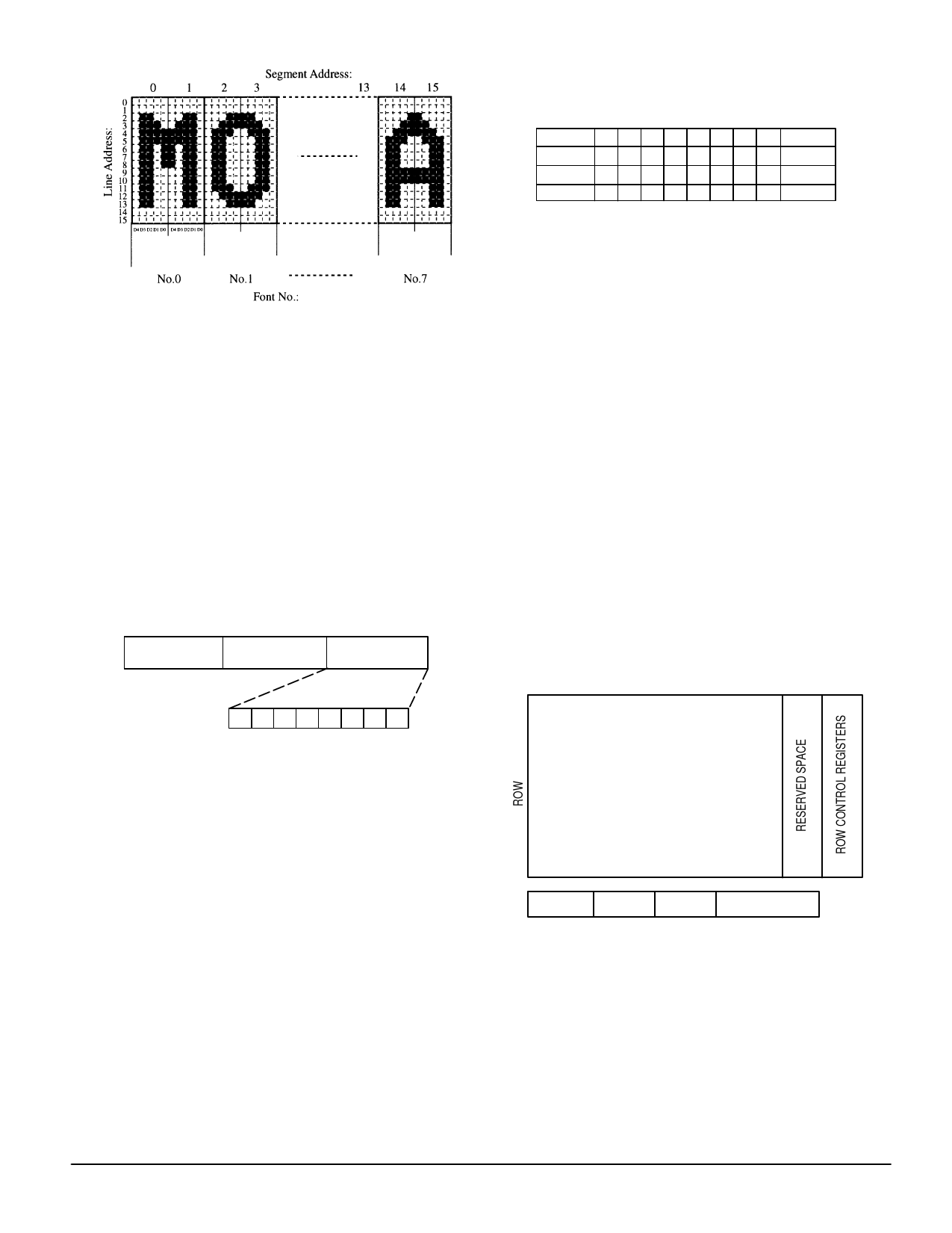
SEG
1 1 X X D D D D a, b, c
ÎÎÎÎÎÎÎÎÎÎÎÎÎ LINE
0 0 X X D D D D a, b
ÎÎÎÎÎÎÎÎÎÎÎÎÎ LINE
0 1 XXDDD D c
ÎÎÎÎÎÎÎÎÎÎÎÎÎ X: don’t care
D: valid data
Figure 7. Segment and Line Address Bit Patterns
Figure 5. Segment Address Structure
Basically, the transmission format is very similar to that for
display RAM or control registers. The major difference is to
replace the row and column address with segment address
and line address, respectively. After the proper identification
by the receiving device, a data train of arbitrary length is
transmitted from the master.
There are three transmission formats, from (a) to (c) as
stated below. The data train in each sequence consists of
segment adress (S), line address (L), and font information (I),
as shown in Figure 6. In format (a), each font information
data has to be preceded with the corresponding segment ad-
dress and line address. This format is particularly suitable for
updating small portions of font patterns. However, if the cur-
rent information byte has the same segment address as the
one before, format (b) is recommended.
ÎÎÎÎÎÎÎÎÎÎÎÎÎÎÎÎÎÎÎÎÎÎÎÎÎÎ SEGADDRESS LINEADDRESS INFORMATION
X X X D4 D3 D2 D1 D0
NOTE: X means don’t care bit and D means valid data bit.
Figure 6. Data Packet
For a new font pattern change which requires a massive
information update, or during power–up, most of the segment
and column address on either format (a) or (b) will appear to
be redundant. A more efficient data transmission format (c)
should be applied. It sends the character RAM starting seg-
ment and line addresses only once, and then treats all sub-
sequent data as font information. The segment and line
addresses will be automatically incremented internally for
each RAM font data from the starting location.
The data transmission formats are:
(a) S – > L– > I – > S – > L – > I – > . . . . . . . . .
(b) S – > L – > I – > L – > I – > L – > I. . . . . . .
(c) S – > L – > I – > I – > I – > . . . . . . . . . . . . .
To differentiate the segment address from row and line ad-
dresses when transferring data, Bit 7 (MSB) and Bit 6 are
set, as in Figure 7, to ‘11’ to represent segment address, or
‘00’ to represent line address in format (a) or (b), or ‘01’ to
represent line address in format (c). However, there is some
limitation on using mixed formats during a single transmis-
sion. It is permissible to change the format from (a) to (b), or
MC141541
6
MEMORY MANAGEMENT
Inside this chip there are three kinds of RAM: display
RAM, control registers, and character RAM. Display RAM
and control registers are addressed with row and column
(coln) number in sequence, while the character RAM is ad-
dressed with segment and line number. The transmission
format is described in the Data Transmission Formats sec-
tion. In addition to the eight RAM fonts numbered from $00 to
$07, 120 masked ROM fonts numbered from $08 to $7F are
also built in to this chip.
Display RAM and Control Registers
The spaces between Row 0 and Coln 0 to Row 9 and Coln
23 are called display registers, and each contains a charac-
ter RAM/ROM number corresponding to a display location on
the monitor screen. Every data row is associated with two
control registers, located at Coln 30 and 31 of their respec-
tive rows, that control the character display format for that
row. In addition, three window control registers for each of
three windows, together with three frame control registers,
occupy the first 13 columns of Row 10.
0
9
ÎÎÎÎÎÎÎÎ00 ÎÎÎÎÎÎÎÎÎÎÎÎÎÎÎÎ2 ÎÎÎÎÎÎÎÎ3 DÎÎÎÎÎÎÎÎISPLAÎÎÎÎÎÎÎÎ5CYO6RLEÎÎÎÎÎÎÎÎUGMISNTÎÎÎÎÎÎÎÎER8SÎÎÎÎÎÎÎÎ9 ÎÎÎÎÎÎÎÎÎÎÎÎÎÎÎÎ23 2ÎÎÎÎÎÎÎÎ4... 12ÎÎÎÎÎÎÎÎ29 30ÎÎÎÎÎÎÎÎ31ÎÎÎÎÎÎÎÎ
10 WINDOW 1 WINDOW 2 WINDOW 3 FRAME CRTL REG
WINDOW AND FRAME CONTROL REGISTERS
Figure 8. Memory Map
The user should handle the internal RAM address location
with care, especially those rows with double length alphanu-
meric symbols. For example, if Row n is destined to be
double height on the memory map, the data displayed on
screen Rows n and n+1 will be represented by the data con-
tained in the memory address of Row n only. The data of the
next Row n+1 on the memory map will appear on the screen
as n+2 and n+3 row space, and so on. Hence, it is not neces-
sary to load a row of blank data to compensate for the double
row. The user should minimize excessive rows of data in
MOTOROLA
Share Link: 