MC141541 Ver la hoja de datos (PDF) - Motorola => Freescale
Número de pieza
componentes Descripción
Fabricante
MC141541 Datasheet PDF : 16 Pages
| |||
The bottom half of the Block Diagram contains the hard-
ware functions for the entire system. It performs all the
EMOSD functions such as programmable vertical length
(from 16 lines to 63 lines), display clock generation (which is
phase locked to the incoming horizontal sync signal at Pin 5
HFLB), bordering or shadowing, and multiple windowing.
COMMUNICATION PROTOCOLS
M_BUS Serial Communication
This is a two–wire serial communication link that is fully
compatible with the IIC bus system. It consists of an SDA bi-
directional data line and an SCL clock input line. Data is sent
from a transmitter (master) to a receiver (slave) via the SDA
line, and is synchronized with a transmitter clock on the SCL
line at the receiving end. The maximum data rate is limited to
100 kbps and the default chip address is $7A, but is hard-
ware changeable by mask set.
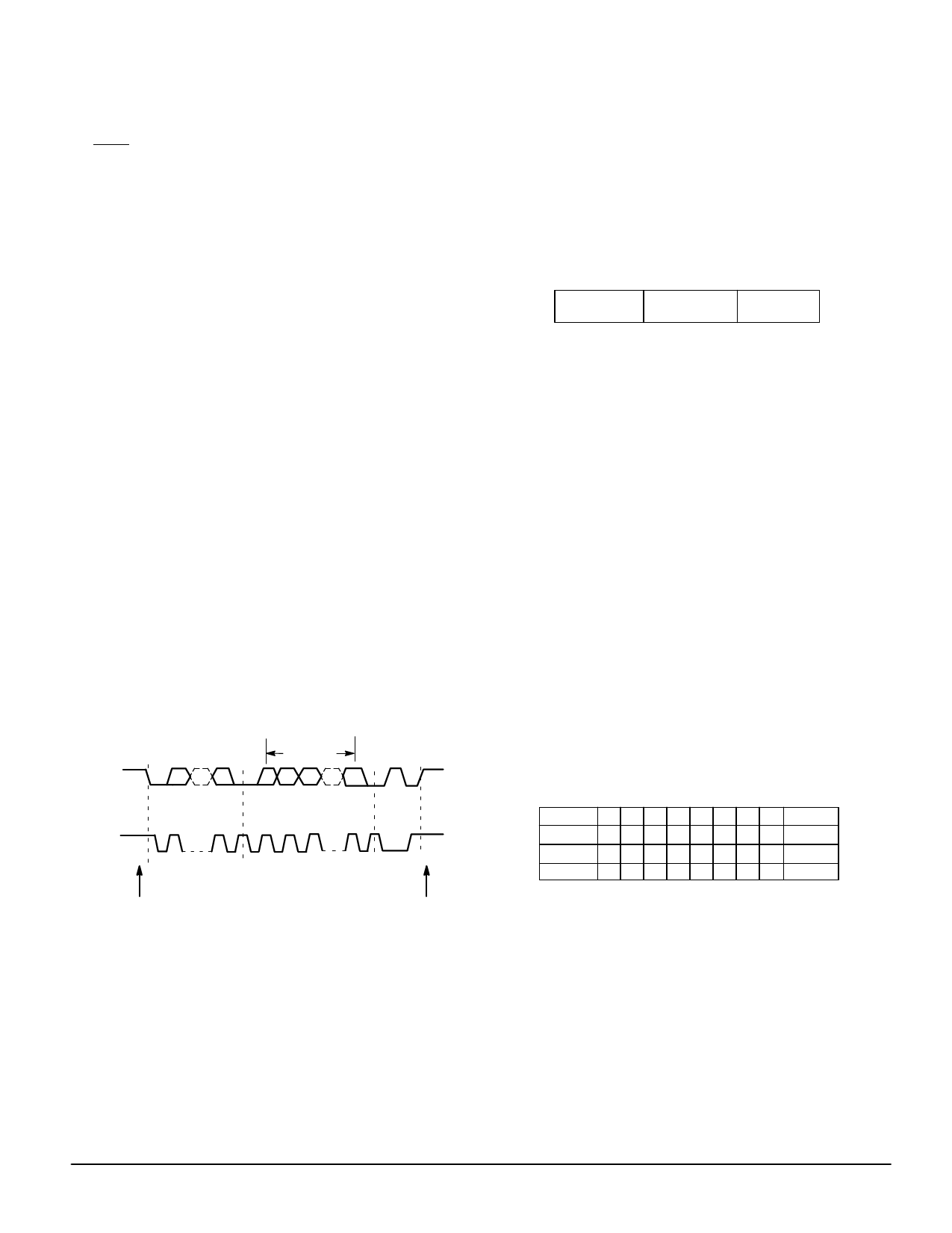
Operating Procedure
Figure 2 shows the M_BUS transmission format. The mas-
ter initiates a transmission routine by generating a start
condition followed by a slave address byte. Once the ad-
dress is properly identified, the slave will respond with an ac-
knowledge signal by pulling the SDA line low during the ninth
SCL clock. Each data byte that follows must be eight bits
long, plus the acknowledge bit, for a total of nine bits. Ap-
propriate row and column address information and display
data can be downloaded sequentially in one of the three
transmission formats described in the Data Transmission
Formats section. In the cases of no acknowlege or comple-
tion of data transfer, the master will generate a stop condition
to terminate the transmission routine. Note that the OSD_EN
bit must be set after all the display information has been sent,
in order to activate the EMOSD circuitry of MC141541 so that
the received information can be displayed.
CHIP ADDRESS
SDA
ACK
DATA BYTES
ACK
SCL
1 2–7 8 9
START CONDITION
STOP CONDITION
Figure 2. M_BUS Format
DATA TRANSMISSION FORMATS
In this enhanced version MOSD, both display RAM, con-
trol registers, and character RAM fonts need to be pro-
grammed after power–on. The arrangement of the display
RAM and control registers is on the row–column basis, while
the character RAM is on the segment–line basis. Although
the address basis is different, the data downloading proto-
cols are very similar and will be described in the following
sections.
Display RAM and Control Registers
After the proper identification by the receiving device, a
data train of arbitrary length is transmitted from the master.
There are three transmission formats from (a) to (c) as stated
below. The data train in each sequence consists of row ad-
dress (R), column address (C), and display information (I), as
shown in Figure 3. In format (a), display information data
must be preceded with the corresponding row address and
column address. This format is particularly suitable for updat-
ing small amounts of data between different rows. However,
if the current information byte has the same row address as
the one before, format (b) is recommended.
ÎÎrÎÎowadÎÎdr ÎÎÎÎcÎÎoladdÎÎr ÎÎÎÎinfÎÎo ÎÎÎÎ
Figure 3. Data Packet
For a full–screen pattern change that requires a massive
information update, or during power–up, most of the row and
column addresses of either (a) or (b) formats will be consec-
utive. Therefore, a more efficient data transmission format (c)
should be applied. This sends the RAM starting row and col-
umn addresses once only, and then treats all subsequent
data as display information. The row and column addresses
will be automatically incremented internally for each display
information data from the starting location.
The data transmission formats are:
(a) R – > C – > I – > R – > C – > I – > . . . . . . . . .
(b) R – > C – > I – > C – > I – > C – > I. . . . . . .
(c) R – > C – > I – > I – > I – > . . . . . . . . . . . . .
To differentiate the row and column addresses when trans-
ferring data from master, the MSB (most significant bit) is set,
as in Figure 4: ‘1’ to represent row, and ‘0’ for column ad-
dress. Furthermore, to distinguish the column address be-
tween formats (a), (b), and (c), the sixth bit of the column
address is set to ‘1’ which represents format (c), and ‘0’ for
format (a) or (b). However, there is some limitation on using
mixed formats during a single transmission. It is permissible
to change the format from (a) to (b), or from (a) to (c), or from
(b) to (a), but not from (c) back to (a) or (b).
ADDRESS
ÎÎÎÎÎÎÎÎÎÎÎÎÎÎ 7
ÎÎÎÎÎÎÎÎÎÎÎÎÎÎ ROW
1
ÎÎÎÎÎÎÎÎÎÎÎÎÎÎ COLUMN 0
ÎÎÎÎÎÎÎÎÎÎÎÎÎÎ COLUMN 0
BIT
654321
XX X D DD
0 XDDDD
1 XDDDD
FORMAT
0
D a, b, c
D a, b
Dc
X: don’t care
D: valid data
Figure 4. Row & Column Address Bit Patterns
Character RAM
The structure of eight character RAM fonts is shown in Fig-
ure 5. They occupy the font number from 0 to 7. Because of
the 10 x 16 dot matrix font, each font is broken down into two
segments in the horizontal direction and 16 lines in the verti-
cal direction. Therefore, there are five dots that need to be
defined for each specified segment–line location. This 5–bit
data forms the lower five bits of the information data byte and
the higher three bits are ignored. Because there are 16 seg-
ments (two segments per font) and 16 lines, both the seg-
ment and line addresses are four bits wide.
MOTOROLA
MC141541
5
Share Link: 