MC13001XP Ver la hoja de datos (PDF) - Motorola => Freescale
Número de pieza
componentes Descripción
Fabricante
MC13001XP Datasheet PDF : 10 Pages
| |||
MC13001X MC13007X
GENERAL DESCRIPTION
The Video IF Amplifier is a four–stage design with 80 µV,
sensitivity. It uses a 6.2 V supply decoupled at Pin 4. The first
two stages are gain controlled, and to ensure optimum noise
performance, the first stage control is delayed until the
second stage has been gain reduced by 15 dB. To bias the
amplifier, balanced dc feedback is used which is decoupled
at Pins 2 and 6 and then fed to the input Pins 3 and 5 by
internal 3.9 k resistors. The nominal bias voltage at these
input pins is approximately 4.2 Vdc. The input, because of the
high IF gain, should be driven from a balanced differential
source. For the same reason, care must be taken with the IF
decoupling.
The IF output is rectified in a full wave envelope detector
and detector nonlinearity is compensated by using a similar
nonlinear element in a feedback output buffer amplifier. The
detected 1.9 Vpp video at Pin 28 contains the sound
intercarrier signal, and Pin 28 is normally used as the sound
takeoff point. The video frequency response, detector to Pin
28, is shown in Figure 3 and the detector intermodulation
performance can be seen by reference to Figure 4. Typical
Pin 28 video waveforms and voltage levels are shown in
Figure 5.
The video processing section of Monomax contains a
contrast control, black level clamp, a beam current limiter and
composite blanking. The video signal first passes through the
contrast control. This has a range of 14:1 for a 0 V to 5.0 V
change of voltage on Pin 26, which corresponds to a change
of video amplitude at Pin 24 of 1.4 V to 0.1 V (black to white
level). The beam current limiter operates on the contrast
control, reducing the video signal when the beam current
exceeds the limit set by external components. As the beam
current increases, the voltage at Pin 27 moves negatively
from its normal value of 1.5 V, and at 1.0 V operates the
contrast control, thus initiating beam limiting action. After the
contrast control, the video is passed through a buffer amplifier
and dc is restored by the black level clamp circuit before
being fed to Pin 24 where it is blanked. The black level clamp,
which is gated “on” during the second half of the flyback,
maintains the video black level at 2.4 V ± 0.1 V under all
conditions, including changes in contrast, temperature and
power supply. The loop integrating capacitor is at Pin 25 and
is normally at a voltage of 3.3 V. The frequency response of
the video at Pin 24 is shown in Figure 3 and it is blanked to
within 0.5 V of ground.
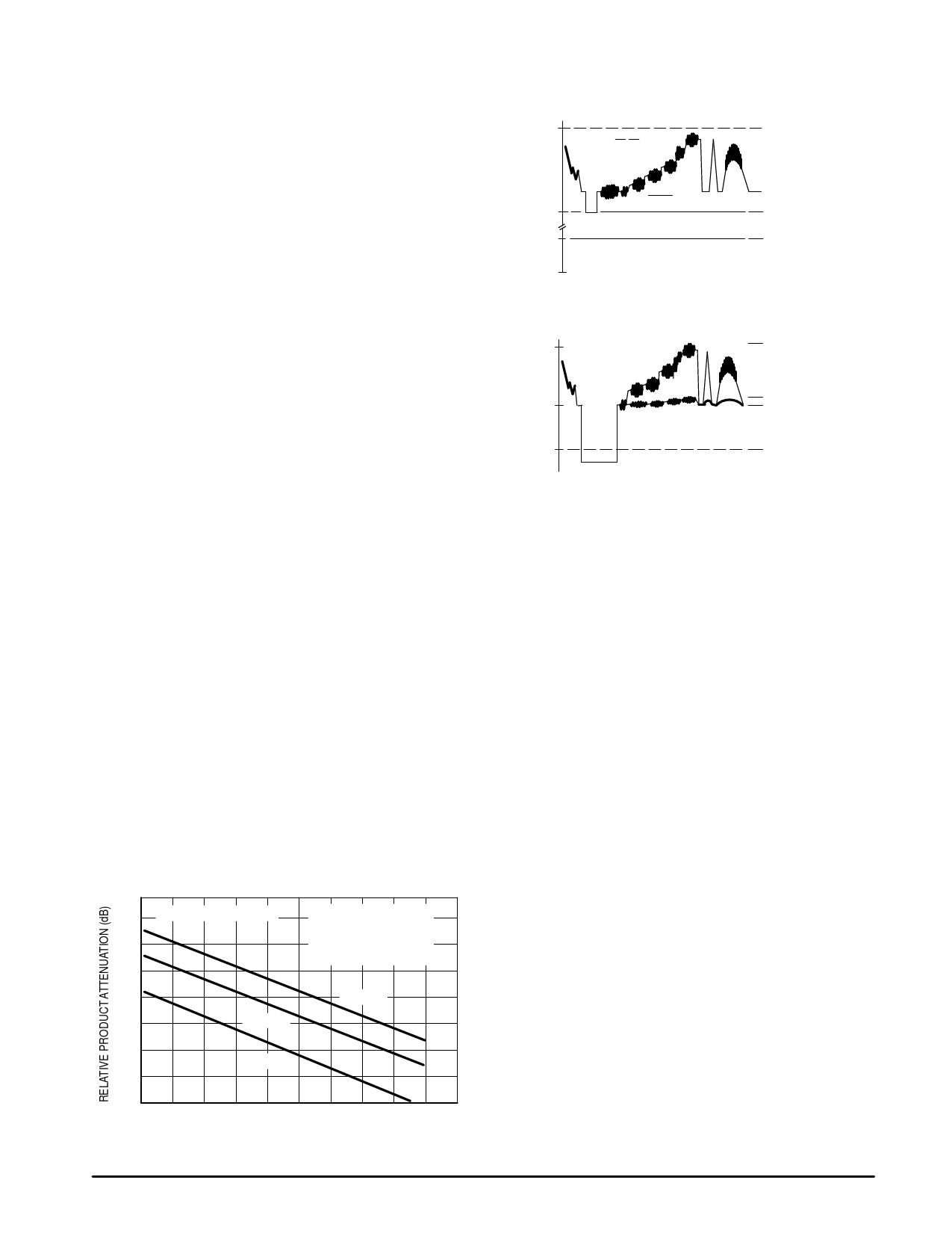
Figure 4. Detector Products
10
0 – Reference = 3.58 MHz
–10
–20
45.74 MHz = 25 mVrms
42.17 MHz = 12.5 mVrms
41.25 MHz = Relative to
41.25 MHz = 45.75 MHz
–30
4.5 MHz
–40
920 kHz
–50
2.66 MHz
–60
–10
–20
–30
–40
–50
RELATIVE 41.25 MHz INPUT LEVEL (dB)
Figure 5. Pin 28 Sound Output
7.0 V
87.5%
Zero Carrier
25%
Back Porch
5.1 V
AGC Threshold
3.6 V
Noise Threshold
Figure 6. Pin 24 Video Output
3.8V
Max. Contrast
2.4V
Min. Contrast
Back Porch
1.7V
Max. Blanking Level
The AGC loop is a gated system, and for all normal
variations of the IF input signal, maintains the sync tip of a
noise filtered video signal at a reference voltage (5.1 V
Pin 28). The strobe for the AGC error amplifier is formed by
gating together the flyback pulse with the separated sync
pulse. Integration of the error signal is performed by the
capacitor at Pin 8, which forms the dominant AGC time
constant. Improved noise performance is obtained by the use
of a gated AGC system, noise protected by a dc coupled
noise canceling circuit. The false AGC lock conditions, which
can result from this combination, are prevented by an
anti–lockout circuit connected to the sync separator at Pin 7.
AGC lockout conditions, which occur due to large rapid
changes of signal level are detected at Pin 7 and recovery is
ensured under these conditions by changing the AGC into a
mean level system. The voltage at Pin 10 sets the point at
which tuner AGC takeover occurs and positive going tuner
control, suitable for an NPN RF transistor, is available at
Pin 11. The maximum output is 5.5 V at 5.0 mA. A
feed–forward output is provided at Pin 9. This enables the
AGC control voltage to be ac coupled into the tuner takeover
control at Pin 10. The coupling allows additional IF gain
reduction during signal transient conditions, thus
compensating for variations of AGC loop gain at the tuner
AGC takeover point. In this way the AGC system stability and
response are not degraded.
The previously mentioned noise protection is effected by
detecting negative–going noise spikes at the video detector
output. A dc coupled detector is used which turns on when a
noise spike exceeds the video sync tip by 1.4 V. This pulse is
then stretched and used to cancel the noise present on the
delayed video at the input to the sync separator. Cancellation
is performed by blanking the video to ground. Complete
cancellation of the noise spike results from the stretching of
the blanking pulse and the delay of the noise spike at the
input to the sync separator. Protection of both the horizontal
PLL and the AGC stems from the fact that both circuits use
the noise cancelled sync for gating.
4
MOTOROLA ANALOG IC DEVICE DATA
Share Link: 