MC100EP116 Ver la hoja de datos (PDF) - ON Semiconductor
Número de pieza
componentes Descripción
Fabricante
MC100EP116 Datasheet PDF : 11 Pages
| |||
MC10EP116, MC100EP116
3.3 V / 5 V Hex Differential
Line Receiver/Driver
Description
The MC10EP116/100EP116 is a 6-bit differential line receiver
based on the EP16 device. The 3.0 GHz bandwidth provided by the
high frequency outputs makes the device ideal for buffering of very
high speed oscillators.
The VBB pin, an internally generated voltage supply, is available to
this device only. For single−ended input conditions, the unused
differential input is connected to VBB as a switching reference voltage.
VBB may also rebias AC coupled inputs. When used, decouple VBB
and VCC via a 0.01 mF capacitor and limit current sourcing or sinking
to 0.5 mA. When not used, VBB should be left open.
The design incorporates two stages of gain, internal to the device,
making it an excellent choice for use in high bandwidth amplifier
applications.
The differential inputs have internal clamp structures which will
force the Q output of a gate in an open input condition to go to a LOW
state. Thus, inputs of unused gates can be left open and will not affect
the operation of the rest of the device. Note that the input clamp will
take affect only if both inputs fall 2.5 V below VCC.
The 100 Series contains temperature compensation.
Features
• 260 ps Typical Propagation Delay
• Maximum Frequency > 3 GHz Typical
• PECL Mode Operating Range: VCC = 3.0 V to 5.5 V
with VEE = 0 V
• NECL Mode Operating Range: VCC = 0 V
with VEE = −3.0 V to −5.5 V
• Open Input Default State
• Safety Clamp on Inputs
• Q Output Will Default LOW with Inputs Open or at VEE
• VBB Output
• Pb−Free Packages are Available
http://onsemi.com
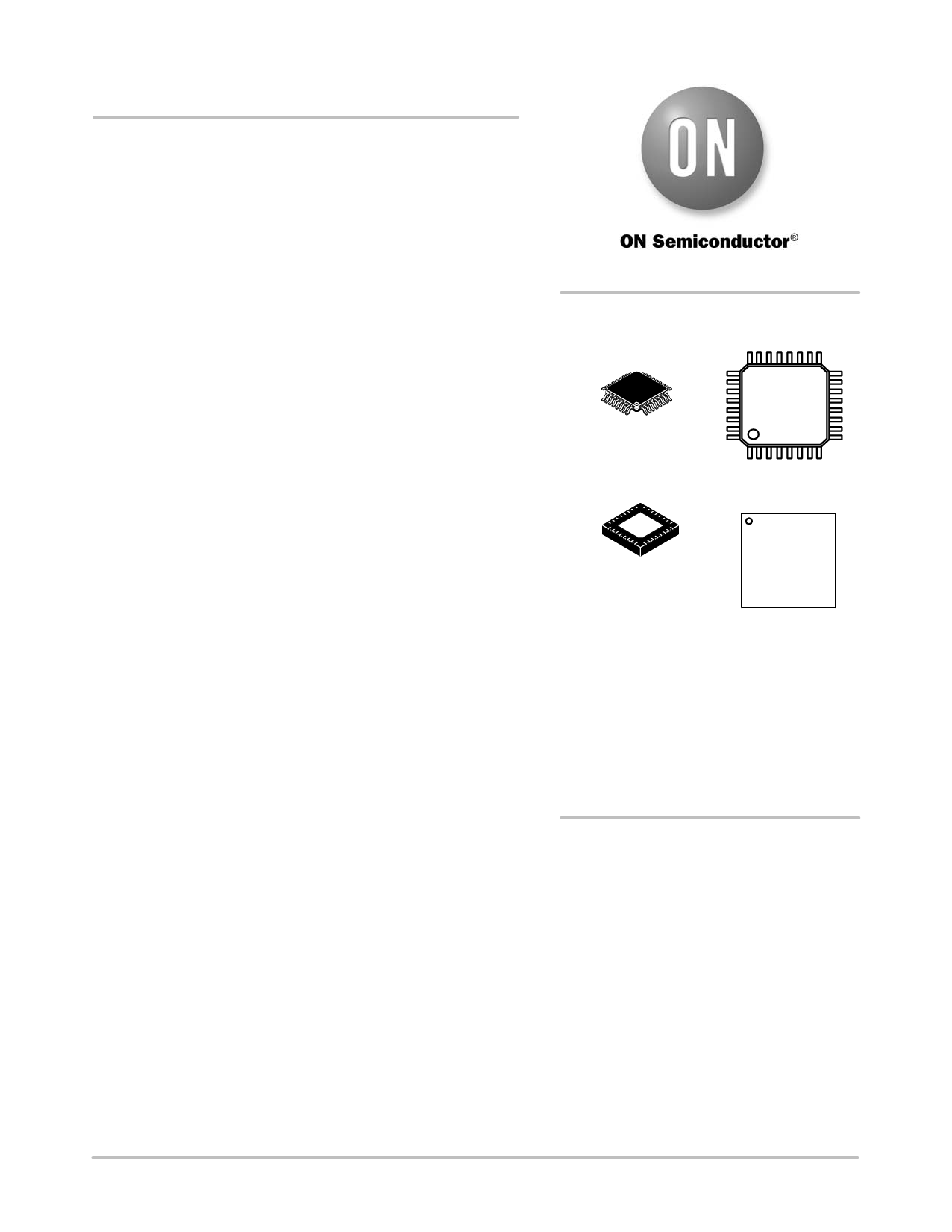
MARKING
DIAGRAM*
LQFP−32
FA SUFFIX
CASE 873A
MCxxx
EP116
AWLYYWWG
1 32
QFN32
MN SUFFIX
CASE 488AM
1
MCxxx
EP116
AWLYYWWG
G
xxx = 10 or 100
A
= Assembly Location
WL, L = Wafer Lot
YY, Y = Year
WW, W = Work Week
G or G = Pb−Free Package
(Note: Microdot may be in either location)
*For additional marking information, refer to
Application Note AND8002/D.
ORDERING INFORMATION
See detailed ordering and shipping information in the package
dimensions section on page 9 of this data sheet.
© Semiconductor Components Industries, LLC, 2006
1
December, 2006 − Rev. 11
Publication Order Number:
MC10EP116/D
Share Link: 