MC100E175FNR2 Ver la hoja de datos (PDF) - ON Semiconductor
Número de pieza
componentes Descripción
Fabricante
MC100E175FNR2 Datasheet PDF : 8 Pages
| |||
MC10E175, MC100E175
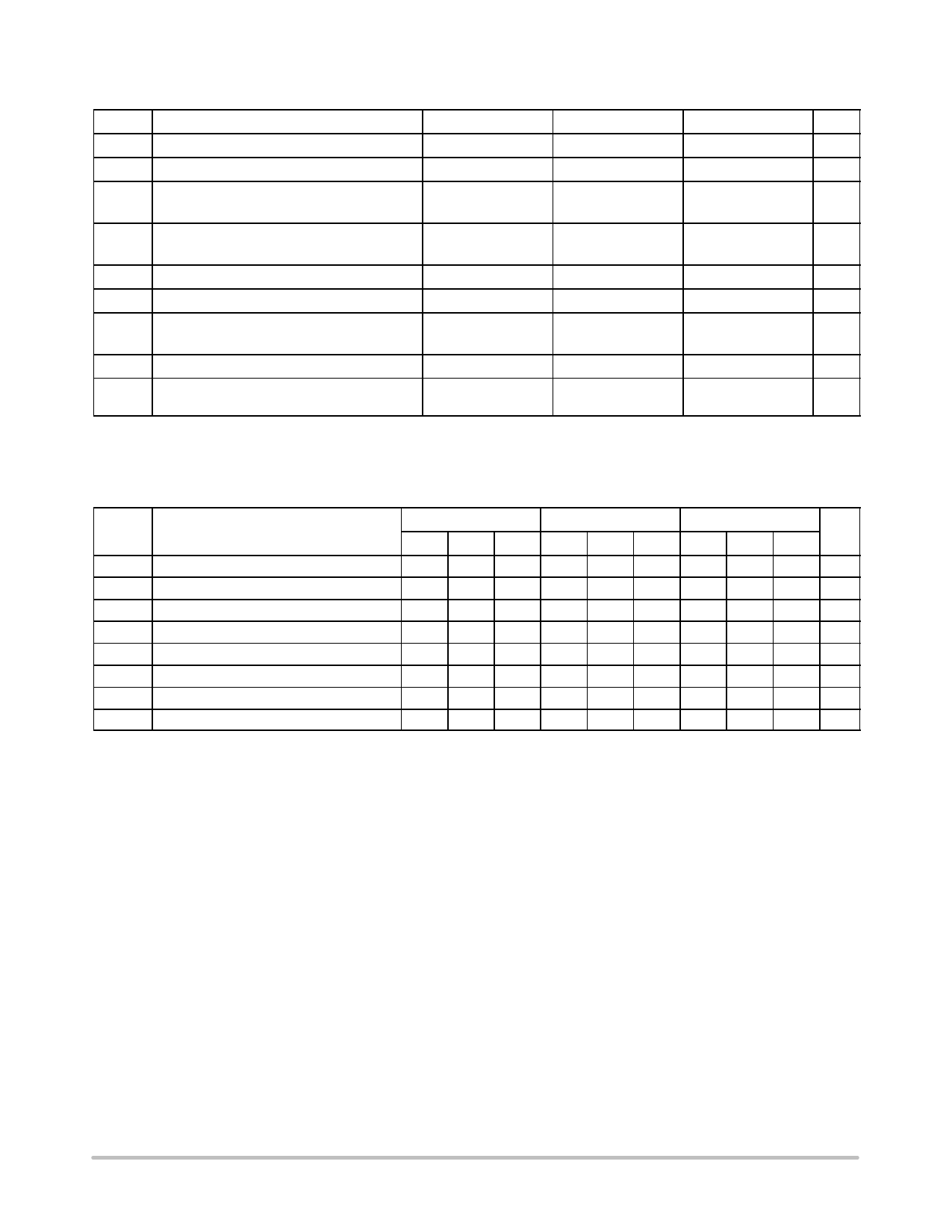
Table 3. MAXIMUM RATINGS
Symbol
Parameter
Condition 1
Condition 2
Rating
Unit
VCC
PECL Mode Power Supply
VEE
NECL Mode Power Supply
VI
PECL Mode Input Voltage
NECL Mode Input Voltage
Iout
Output Current
VEE = 0 V
VCC = 0 V
VEE = 0 V
VCC = 0 V
Continuous
Surge
VI v VCC
VI w VEE
8
V
−8
V
6
V
−6
V
50
mA
100
mA
TA
Operating Temperature Range
Tstg
Storage Temperature Range
qJA
Thermal Resistance (Junction−to−Ambient) 0 lfpm
500 lfpm
PLCC−28
PLCC−28
0 to +85
−65 to +150
63.5
43.5
°C
°C
°C/W
°C/W
qJC
Thermal Resistance (Junction−to−Case)
Standard Board
Tsol
Wave Solder
Pb
Pb−Free
PLCC−28
22 to 26
265
265
°C/W
°C
Stresses exceeding Maximum Ratings may damage the device. Maximum Ratings are stress ratings only. Functional operation above the
Recommended Operating Conditions is not implied. Extended exposure to stresses above the Recommended Operating Conditions may affect
device reliability.
Table 4. 10E SERIES PECL DC CHARACTERISTICS VCCx = 5.0 V, VEE = 0.0 V (Note 1)
0°C
25°C
85°C
Symbol
Characteristic
Min Typ Max Min Typ Max Min Typ Max Unit
IEE
Power Supply Current
IEE
Power Supply Current
VOH
Output HIGH Voltage (Note 2)
VOL
Output LOW Voltage (Note 2)
VIH
Input HIGH Voltage
VIL
Input LOW Voltage
IIH
Input HIGH Current
IIL
Input LOW Current
94 113
94 113
94 113 mA
110 132
110 132
110 132 mA
3980 4070 4160 4020 4105 4190 4090 4185 4280 mV
3050 3210 3370 3050 3210 3370 3050 3227 3405 mV
3830 3995 4160 3870 4030 4190 3940 4110 4280 mV
3050 3285 3520 3050 3285 3520 3050 3302 3555 mV
150
150
150 mA
0.5 0.3
0.5 0.25
0.3 0.2
mA
NOTE: Device will meet the specifications after thermal equilibrium has been established when mounted in a test socket or printed circuit
board with maintained transverse airflow greater than 500 lfpm. Electrical parameters are guaranteed only over the declared
operating temperature range. Functional operation of the device exceeding these conditions is not implied. Device specification limit
values are applied individually under normal operating conditions and not valid simultaneously.
1. Input and output parameters vary 1:1 with VCC. VEE can vary −0.46 V / +0.06 V.
2. Outputs are terminated through a 50 W resistor to VCC − 2.0 V.
http://onsemi.com
3
Share Link: 