MB88141A Ver la hoja de datos (PDF) - Fujitsu
Número de pieza
componentes Descripción
Fabricante
MB88141A Datasheet PDF : 22 Pages
| |||
MB88141A
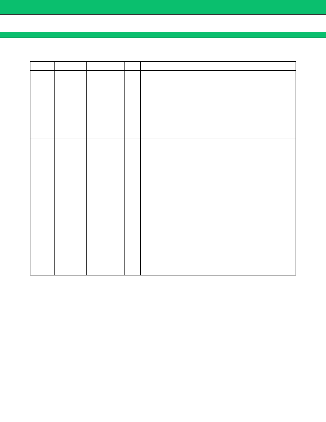
s PIN DESCRIPTION
Pin no. Symbol Circuit Type I/O
Description
21
SDA
C
I/O
I2C bus data input/output pin (hysteresis input).
Outputs the acknowledge signal.
20
SCL
B
I I2C bus shift clock input pin (hysteresis input) .
19
MOD
D/A converter and I/O expander mode switching pin. *1, *2
A
I Input “L” to operate as a D/A converter, “H” to operate as I/O
expander and D/A converter.
16
CS0
17
CS1
18
CS2
These pins set the lower 3 bits of the slave address. *1
A
I This allows up to eight MB88141A chips to be used on the same
bus line.
1
AO1
2
AO2
3
AO3
4
AO4
D
O 8-bit D/A outputs with OP Amp. *2
5
AO5/D7
6
AO6/D6
7
AO7/D5
8
AO8/D4
9
AO9/D3
10
AO10/D2
E
8-bit D/A outputs with OP Amp. *2
I/O In I/O expander operation, these pins function as parallel data in-
put/output pins.
11
AO11/D1
12
AO12/D0
13
VCC Power supply Power supply pin for digital circuits and OP Amp.
24
GND
GND
GND pin for digital circuits and OP Amp.
22
VDD1 Power supply Reference power supply pin for D/A converter (H) . AO1 to AO4.
23
VSS1 Power supply Reference power supply pin for D/A converter (L) . AO1 to AO4.
15
VDD2 Power supply Reference power supply pin for D/A converter (H) . AO5 to AO12.
14
VSS2 Power supply Reference power supply pin for D/A converter (L) . AO5 to AO12.
*1: The MOD and CS0-CS2 pins should be used with fixed level input.
*2: When using the I/O expander function together with the D/A converter function, take care that D/A converter
output precision is within a range that will not affect overall system operation.
4
Share Link: 