MAX9963BGCCQ Ver la hoja de datos (PDF) - Maxim Integrated
Número de pieza
componentes Descripción
Fabricante
MAX9963BGCCQ Datasheet PDF : 25 Pages
| |||
Quad, Low-Power, 500Mbps
ATE Driver/Comparator
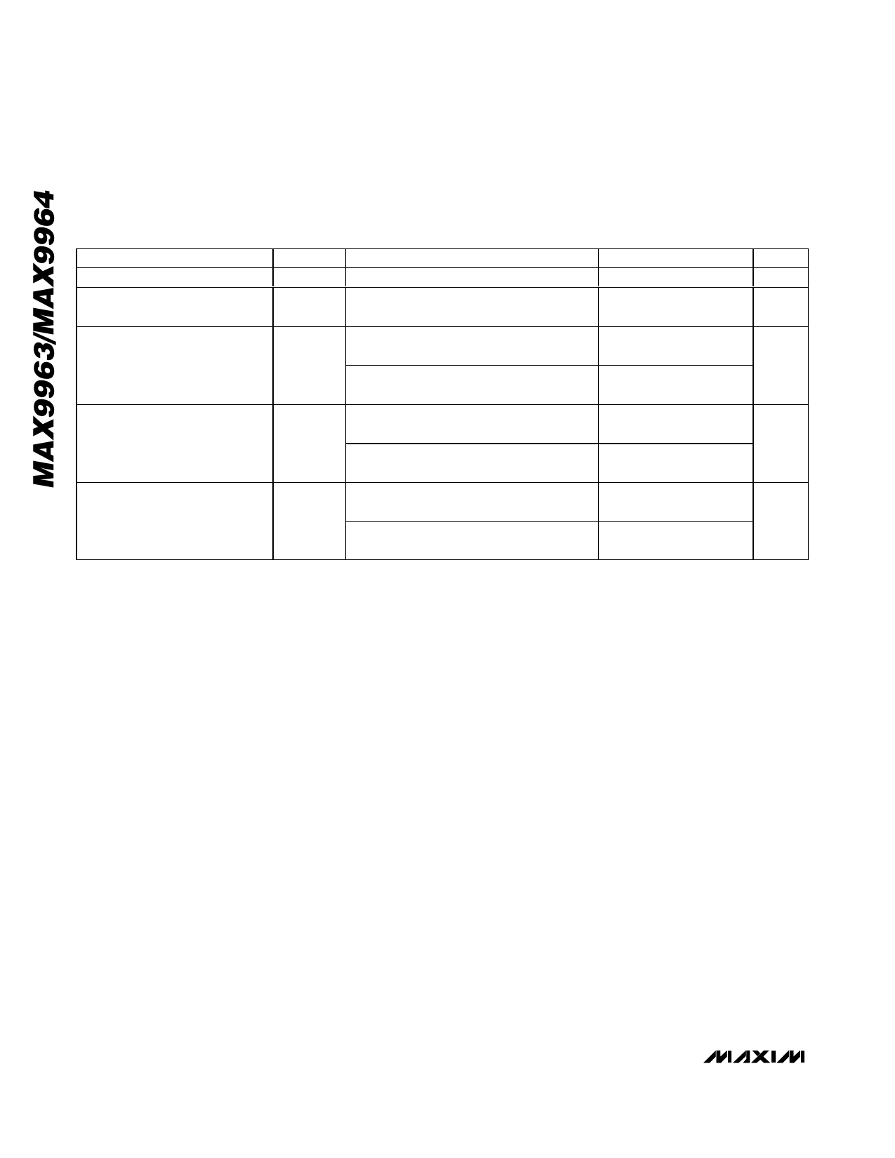
ELECTRICAL CHARACTERISTICS (continued)
(VCC = +9.75V, VEE = -5.25V, VCCO_ _ = 2.5V, SC1 = SC0 = 0, VCPHV_ = 7.2V, VCPLV_ = -2.2V, TJ = +85°C, unless otherwise noted. All tem-
perature coefficients are measured at TJ = +70°C to +100°C, unless otherwise noted.) (Note 1)
PARAMETER
Voltage Gain
Voltage-Gain Temperature
Coefficient
SYMBOL
AV
CONDITIONS
MIN TYP MAX UNITS
0.96
1.00
V/V
-100
ppm/°C
Clamp Linearity
IDUT = 1mA, VCPLV_ = -1.5V, VCPHV_ = -0.3
±10
to 6.5V
mV
IDUT = -1mA, VCPHV_ = 6.5V, VCPLV_ = -1.5
to 5.3V
±10
Short-Circuit Output Current
VCPHV_ = 0, VCPLV_ = -1.5V,
VDUT_ = 6.0V
VCPLV_ = 5V, VCPHV_ = 6.5V,
VDUT_ = -1.0V
50
95
mA
-95
-50
Clamp DC Impedance
VCPHV_ = 3V, VCPLV_ = 0,
IDUT = -5mA and -15mA
VCPHV_ = 3V, VCPLV_ = 0,
IDUT = 5mA and 15mA
50
55
Ω
50
55
Note 1: All MIN and MAX limits are 100% tested in production.
Note 2: Total for quad device at worst-case setting. RL_ ≥ 10MΩ. The applicable supply currents are measured with typical supply
voltages.
Note 3: Does not include internal dissipation of the comparator outputs. With output loads of 50Ω to (VVCCO_ _ - 2V), this adds
240mW (typ) to the total chip power (MAX996_ _HCCQ, MAX996_ _JCCQ).
Note 4: Externally forced voltages may exceed this range provided that the absolute maximum ratings are not exceeded.
Note 5: Transition time from LLEAK being asserted to leakage current dropping below specified limits.
Note 6: Transition time from LLEAK being deasserted to output returning to normal operating mode.
Note 7: Based on simulation results only.
Note 8: With the exception of offset and gain/CMRR tests, reference input values are calibrated for offset and gain.
Note 9: Relative to straight line between 0 and 3V.
Note 10: Full ranges are -1.3V ≤ VDHV_ ≤ 6.5V, -1.5V ≤ VDTV_ ≤ 6.5V, -1.5V ≤ VDLV_ ≤ 6.3V.
Note 11: Nominal target value is 50Ω. Contact factory for alternate trim selections within the 45Ω to 51Ω range.
Note 12: VDTV_ = 1.5V, RS = 50Ω. External signal driven into T-line is a 0 to 3V edge with 1.2ns rise time (10% to 90%).
Measurement is made using the comparator.
Note 13: Measured from the crossing point of DATA_ inputs to the settling of the driver output.
Note 14: Prop delays are measured from the crossing point of the differential input signals to the 50% point of expected output
swing. Rise time of the differential inputs DATA_ and RCV_ is 250ps (10% to 90%).
8 _______________________________________________________________________________________
Share Link: 