MAX8790A Ver la hoja de datos (PDF) - Maxim Integrated
Número de pieza
componentes Descripción
Fabricante
MAX8790A
Maxim Integrated

MAX8790A Datasheet PDF : 22 Pages
| |||
MAX8790A
Six-String White LED Driver with Active
Current Balancing for LCD Panel Applications
Absolute Maximum Ratings
IN, SHDN, to GND..................................................-0.3V to +28V
Operating Temperature Range.............................-40°C to +85°C
FB_ to GND............................................................-0.3V to +28V
Junction Temperature.......................................................+150°C
VCC, BRT, ENA, OSC, OV to GND...........................-0.3V to +6V
ISET, CCV, CS, FSET, CPLL, EXT to GND .-0.3V to (VCC + 0.3V)
Continuous Power Dissipation (TA = +70°C)
TQFN (derate 16.9mW/°C above +70°C)....................1349mW
Storage Temperature Range..............................-60°C to +150°C
Lead Temperature (soldering, 10s)...................................+300°C
Stresses beyond those listed under “Absolute Maximum Ratings” may cause permanent damage to the device. These are stress ratings only, and functional operation of the device at these
or any other conditions beyond those indicated in the operational sections of the specifications is not implied. Exposure to absolute maximum rating conditions for extended periods may affect
device reliability.
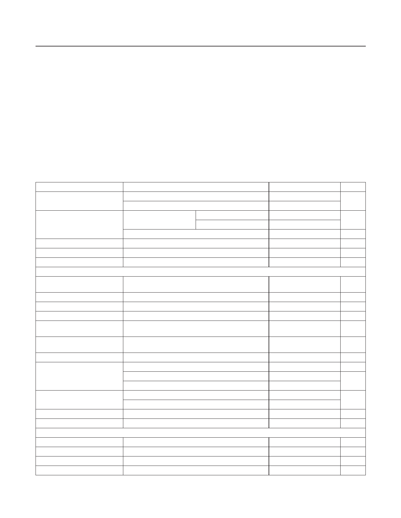
Electrical Characteristics
(Circuit of Figure 1. VIN = 12V, VSHDN = VIN, CCV = 0.1μF, TA = 0°C to +85°C, unless otherwise noted. Typical values are at TA = +25°C.)
PARAMETER
CONDITIONS
MIN TYP MAX UNITS
IN Input Voltage Range
IN Quiescent Current
VIN = VCC
VCC = bypassed to GND through 1µF capacitor
VSHDN = high,
BRT = GND
VIN = 26V
VIN = VCC = 5V
SHDN = GND
4.5
5.5
V
5.5
26.0
1
2
mA
1
2
10
µA
VCC Output voltage
VCC Short-Circuit Current
VCC UVLO Threshold
STEP-UP CONVERTER
VSHDN = 5V, 6V < VIN < 26V, 0 < IVCC < 10mA
Rising edge, hysteresis = 20mV
4.7
5.0
5.3
V
15
56
130
mA
4.00 4.25 4.45
V
EXT High Level
10mA from EXT to GND
VCC -
0.1
VCC
V
EXT Low Level
EXT On-Resistance
-10mA from EXT to VCC
EXT high or low
0
0.1
V
2
5
Ω
EXT Sink/Source Current
EXT forced to 2V
1
A
OSC High-Level Threshold
VCC -
0.4
V
OSC Midlevel Threshold
1.5
VCC -
2.0
V
OSC Low-Level Threshold
0.4
V
Operating Frequency
Minimum Duty Cycle
VOSC = VCC
VOSC = open
VOSC = GND
PWM mode
Pulse skipping, no load
0.9
1.0
1.1
MHz
675
750
825
kHz
450
500
550
10
%
0
Maximum Duty Cycle
94
95
%
CS Trip Voltage
Duty cycle = 75%
85
100
115
mV
CONTROL INPUT
SHDN Logic-Input High Level
2.1
V
SHDN Logic-Input Low Level
0.8
V
BRT, ENA Logic-Input High Level
2.1
V
BRT, ENA Logic-Input Low Level
0.8
V
www.maximintegrated.com
Maxim Integrated │ 2
Share Link: