MAX5580A(2008) Ver la hoja de datos (PDF) - Maxim Integrated
Número de pieza
componentes Descripción
Fabricante
MAX5580A
(Rev.:2008)
(Rev.:2008)
Maxim Integrated

MAX5580A Datasheet PDF : 34 Pages
| |||
Buffered, Fast-Settling, Quad,
12-/10-/8-Bit, Voltage-Output DACs
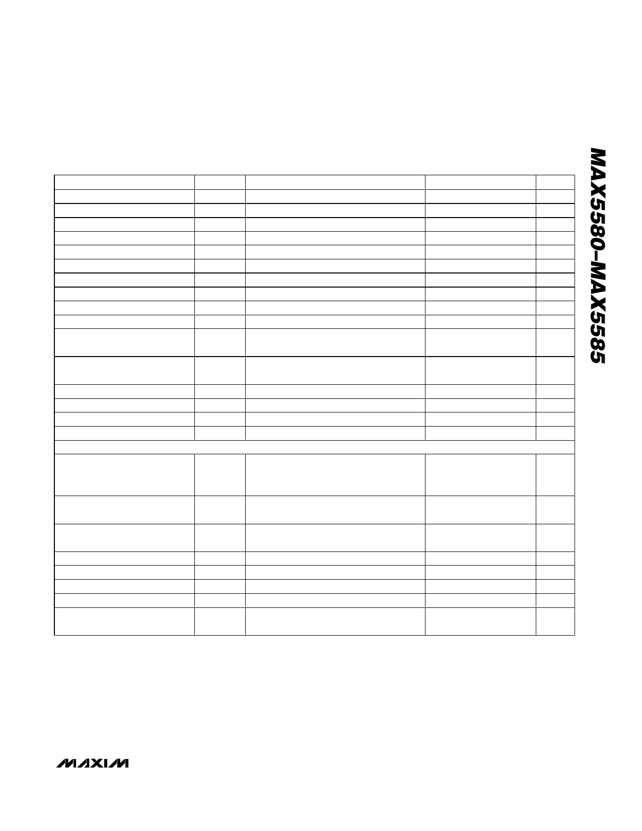
TIMING CHARACTERISTICS—DSP Mode Enabled (1.8V Logic) (Figure 2)
(DVDD = 1.8V to 2.7V, AGND = DGND = 0, TA = TMIN to TMAX, unless otherwise noted.)
PARAMETER
SYMBOL
CONDITIONS
MIN
SCLK Frequency
fSCLK 1.8V < DVDD < 2.7V
SCLK Pulse-Width High
tCH
(Note 7)
40
SCLK Pulse-Width Low
tCL
(Note 7)
40
CS Fall to SCLK Fall Setup Time
tCSS
20
DSP Fall to SCLK Fall Setup Time
tDSS
20
SCLK Fall to CS Rise Hold Time
tCSH
5
SCLK Fall to CS Fall Delay
tCS0
10
SCLK Fall to DSP Fall Delay
tDS0
15
DIN to SCLK Fall Setup Time
tDS
20
DIN to SCLK Fall Hold Time
tDH
5
SCLK Rise to DOUT_ Valid
Propagation Delay
tDO1
CL = 20pF, UPIO_ = DOUTDC1 or DOUTRB
mode
TYP
MAX
10
UNITS
MHz
ns
ns
ns
ns
ns
ns
ns
ns
ns
60
ns
SCLK Fall to DOUT_ Valid
Propagation Delay
tDO2 CL = 20pF, UPIO_ = DOUTDC0 mode
CS Rise to SCLK Fall Hold Time
tCS1 MICROWIRE and SPI modes 0 and 3
20
CS Pulse-Width High
tCSW
90
DSP Pulse-Width High
tDSW
40
DSP Pulse-Width Low
tDSPWL (Note 8)
40
UPIO_ TIMING CHARACTERISTICS
60
ns
ns
ns
ns
ns
DOUT Tri-State Time when
Exiting DOUTDC0, DOUTDC1,
and UPIO Modes
tDOZ
CL = 20pF, from end of write cycle to UPIO_
in high impedance
200
ns
DOUTRB Tri-State Time from CS
Rise
tDRBZ
CL = 20pF, from rising edge of CS to UPIO_
in high impedance
40
ns
DOUTRB Tri-State Enable Time
from 8th SCLK Fall
LDAC Pulse-Width Low
LDAC Effective Delay
CLR, MID, SET Pulse-Width Low
GPO Output Settling Time
GPO Output High-Impedance
Time
tZEN
CL = 20pF, from 8th falling edge of SCLK to
UPIO_ driven out of tri-state
0
tLDL
Figure 5
40
tLDS Figure 6
200
tCMS Figure 5
40
tGP
Figure 6
tGPZ
ns
ns
ns
ns
200
ns
200
ns
Note 7: In some daisy-chain modes, data is required to be clocked in on one clock edge and the shifted data clocked out on the fol-
lowing edge. In the case of a 0.5 clock-period delay, it is necessary to increase the minimum high/low clock times to 25ns
(2.7V) or 50ns (1.8V).
Note 8: The falling edge of DSP starts a DSP-type bus cycle, provided that CS is also active low to select the device. DSP active low and
CS active low must overlap by a minimum of 10ns (2.7V) or 20ns (1.8V). CS can be permanently low in this mode of operation.
_______________________________________________________________________________________ 9
Share Link: