MAX4752 Ver la hoja de datos (PDF) - Maxim Integrated
Número de pieza
componentes Descripción
Fabricante
MAX4752 Datasheet PDF : 11 Pages
| |||
MAX4751/MAX4752/MAX4753
0.9Ω, Low-Voltage, Single-Supply Quad SPST
Analog Switches
Detailed Description
The MAX4751/MAX4752/MAX4753 are low 0.9Ω max (at
V+ = 3V) on-resistance, low-voltage quad analog
switches that operate from a +1.6V to +3.6V single sup-
ply. CMOS construction allows switching analog signals
that are within the supply voltage range (GND to V+).
When powered from a +3V supply, the 0.9Ω (max) RON
allows high continuous currents to be switched in a
variety of applications.
Applications Information
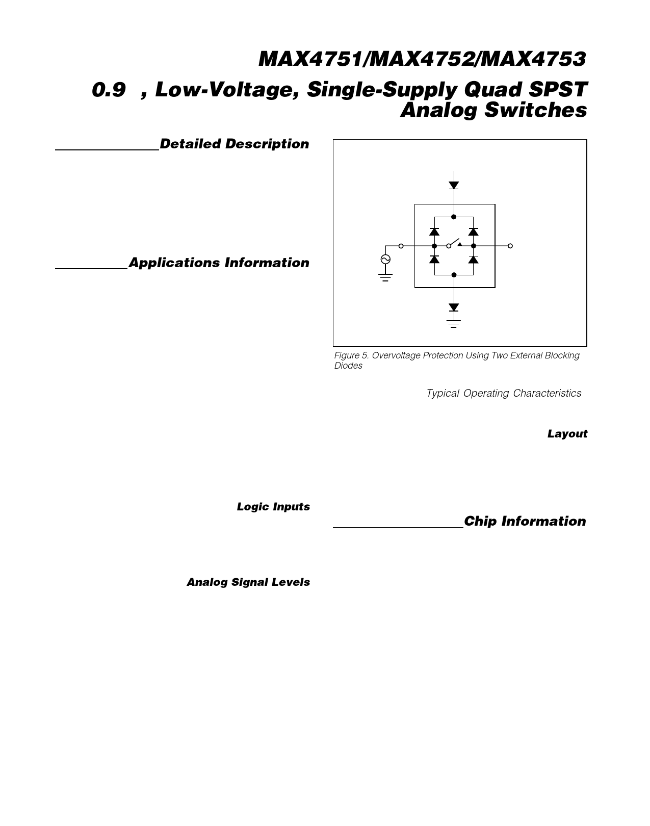
Proper power-supply sequencing is recommended for
all CMOS devices. Do not exceed the absolute maxi-
mum ratings because stresses beyond the listed rat-
ings can cause permanent damage to the devices.
Always sequence V+ on first, followed by NO_, NC_, or
COM_. If power-supply sequencing is not possible, add
two small-signal diodes (D1, D2) in series with the sup-
ply pins for overvoltage protection (Figure 5). Adding
these diodes reduces the analog signal by one diode
drop below V+ and one diode drop above GND, but
does not affect the low switch resistance and low leak-
age characteristics of the device. Device operation is
unchanged, and the difference between V+ and GND
should not exceed 4V.
Power-supply bypassing is needed to improve noise
margin and to prevent switching noise propagation
from the V+ supply to other components. A 0.1µF
capacitor, connected from V+ to GND, is adequate for
most applications.
Logic Inputs
The MAX4751/MAX4752/MAX4753 logic inputs can be
driven up to +3.6V regardless of the supply voltage. For
example, with a +1.8V supply, IN_ may be driven low to
GND and high to +3.6V. Driving IN_ rail-to-rail mini-
mizes power consumption.
Analog Signal Levels
Analog signals that range over the entire supply voltage
(V+ to GND) can be passed with very little change in on-
POSITIVE SUPPLY
D1
V+
MAX4751
MAX4752
MAX4753
COM
NO
Vg
GND
D2
Figure 5. Overvoltage Protection Using Two External Blocking
Diodes
resistance (see the Typical Operating Characteristics).
The switches are bidirectional, so the NO_, NC_, and
COM_ pins can be used as either inputs or outputs.
Layout
High-speed switches require proper layout and design
procedures for optimum performance. Reduce stray
inductance and capacitance by keeping traces short
and wide. Ensure that bypass capacitors are as close
to the device as possible. Use large ground planes
where possible.
Chip Information
TRANSISTOR COUNT: 228
PROCESS: CMOS
Maxim Integrated
9
Share Link: 