MAX475 Ver la hoja de datos (PDF) - Maxim Integrated
Número de pieza
componentes Descripción
Fabricante
MAX475 Datasheet PDF : 12 Pages
| |||
Single/Dual/Quad, 10MHz
Single-Supply Op Amps
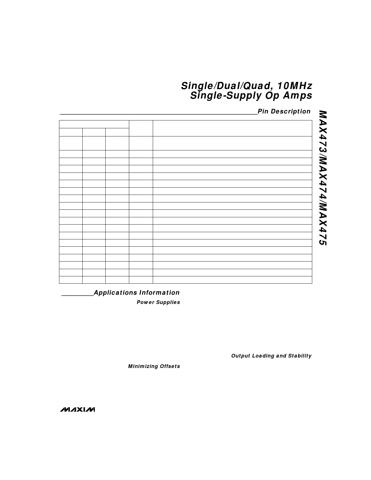
______________________________________________________________Pin Description
PIN
MAX473 MAX474 MAX475
1, 8
—
—
—
1
1
2
—
—
—
2
2
3
—
—
—
3
3
4
4
11
5
—
—
—
5
5
6
—
—
—
6
6
—
7
7
7
8
4
—
—
8
—
—
9
—
—
10
—
—
12
—
—
13
—
—
14
NAME
NULL
OUTA
IN-
INA-
IN+
INA+
VEE
N.C.
INB+
OUT
INB-
OUTB
VCC
OUTC
INC-
INC+
IND+
IND-
OUTD
FUNCTION
Offset Null Input. Connect to one end of 2kΩ potentiometer for offset voltage
trimming. Connect wiper to VEE. See Figure 1.
Amplifier A Output
Inverting Input
Amplifier A Inverting Input
Noninverting Input
Amplifier A Noninverting Input
Negative Power-Supply Pin. Connect to ground or a negative voltage.
No Connect—not internally connected
Amplifier B Noninverting Input
Amplifier Output
Amplifier B Inverting Input
Amplifier B Output
Positive Power-Supply Pin. Connect to (+) terminal of power supply.
Amplifier C Output
Amplifier C Inverting Input
Amplifier C Noninverting Input
Amplifier D Noninverting Input
Amplifier D Inverting Input
Amplifier D Output
__________Applications Information
Power Supplies
The MAX473/MAX474/MAX475 operate from a single
2.7V to 5.25V power supply, or from dual supplies of
±1.35V to ±2.625V. For single-supply operation,
bypass the power supply with 0.1µF. If operating from
dual supplies, bypass each supply to ground. With
0.1µF bypass capacitance, channel separation
(MAX474/MAX475) is typically better than 120dB with
signal frequencies up to 300kHz. Increasing the
bypass capacitance (e.g. 10µF || 0.1µF) maintains
channel separation at higher frequencies.
Minimizing Offsets
The MAX473’s maximum offset voltage is ±2mV
(TA = +25°C). If additional offset adjustment is required,
connect a 2kΩ trim potentiometer between pins 1, 8, and
4 (Figure 1). Input offset voltage for the dual MAX474
and quad MAX475 cannot be externally trimmed.
The MAX473/MAX474/MAX475 are bipolar op amps
with low input bias currents. The bias currents at both
inputs flow out of the device. Matching the resistance
at the op amp’s inputs significantly reduces the offset
error caused by the bias currents. Place a resistor (R3)
from the noninverting input to ground when using the
inverting configuration (Figure 2a); place R3 in series
with the noninverting input when using the noninverting
configuration (Figure 2b). Select R3 such that the paral-
lel combination of R2 and R1 equals R3. Adding R3 will
slightly increase the op amp’s voltage noise.
Output Loading and Stability
The MAX473/MAX474/MAX475 op amps are unity-gain
stable. Any op amp’s stability depends on the configu-
ration, closed-loop gain, and load capacitance. The
unity-gain, noninverting buffer is the most sensitive gain
configuration, and driving capacitive loads decreases
stability.
_______________________________________________________________________________________ 9
Share Link: 