MAX3264 Ver la hoja de datos (PDF) - Maxim Integrated
Número de pieza
componentes Descripción
Fabricante
MAX3264 Datasheet PDF : 17 Pages
| |||
+3.0V to +5.5V, 1.25Gbps/2.5Gbps
Limiting Amplifiers
ABSOLUTE MAXIMUM RATINGS
Supply Voltage (VCC) ............................................-0.5V to +6.0V
Voltage at IN+, IN- ..........................(VCC - 2.4V) to (VCC + 0.5V)
Voltage at SQUELCH, CAZ1,
CAZ2, LOS, LOS, TH..................................-0.5V to (VCC + 0.5V)
Voltage at LEVEL...................................................-0.5V to +2.0V
Current into LOS, LOS ..........................................-1mA to +9mA
Differential Input Voltage (IN+ - IN-) .....................................2.5V
Continuous Current at
CML Outputs (OUT+, OUT-) ..........................-25mA to +25mA
Continuous Current at PECL Outputs (OUT+, OUT-) .........50mA
Continuous Power Dissipation (TA = +70°C)
16-Pin TSSOP (derate 27mW/°C above +70°C) .........2162mW
10-Pin µMAX (derate 20mW/°C above +70°C) ...........1600mW
Operating Ambient Temperature Range .............-40°C to +85°C
Storage Temperature Range .............................-55°C to +150°C
Processing Temperature (dice) .......................................+400°C
Lead Temperature (soldering, 10s) .................................+300°C
Stresses beyond those listed under “Absolute Maximum Ratings” may cause permanent damage to the device. These are stress ratings only, and functional
operation of the device at these or any other conditions beyond those indicated in the operational sections of the specifications is not implied. Exposure to
absolute maximum rating conditions for extended periods may affect device reliability.
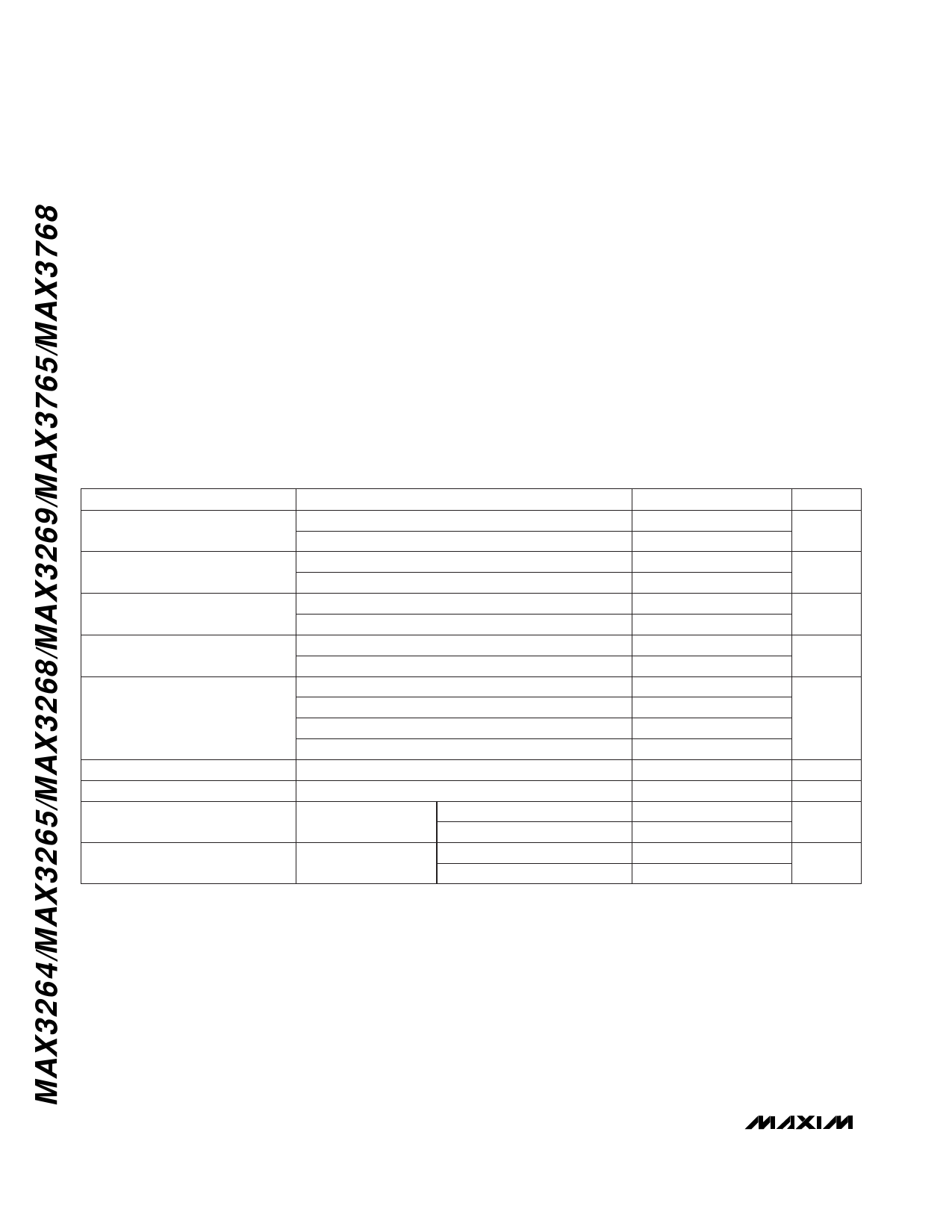
ELECTRICAL CHARACTERISTICS
(Data outputs terminated per Figure 1, VCC = +3.0V to +5.5V, TA = 0°C to +70°C. Typical values are at VCC = +3.3V, TA = +25°C,
unless otherwise noted.) (Note 1)
PARAMETER
CONDITIONS
MIN TYP MAX UNITS
Data Rate
MAX3264/MAX3268/MAX3768
MAX3265/MAX3269/MAX3765
1.25
Gbps
2.5
Input Voltage Range
MAX3264/MAX3268/MAX3768
MAX3265/MAX3269/MAX3765
5
1200
mV
10
1200
Deterministic Jitter
MAX3264/MAX3268/MAX3768 (Notes 2, 3)
MAX3265/MAX3269/MAX3765 (Notes 2, 3)
14
30
psp-p
11
25
Random Jitter
MAX3264/MAX3268/MAX3768 (Notes 2, 4)
MAX3265/MAX3269/MAX3765 (Notes 2, 4)
15
8
psRMS
MAX3264 (Note 5)
80
175
300
Data Output Edge Speed
MAX3265/MAX3765 (Note 6)
MAX3268/MAX3768 (Note 5)
100
150
ps
80
150
300
MAX3269 (Note 6)
100
150
LOS Hysteresis
(Notes 2, 7)
2.5
4.4
dB
LOS Assert/Deassert Time
(Notes 7, 8)
1
µs
MAX3264/MAX3268/MAX3768 1.20
2.6
Low LOS Assert Level
RTH = 2.5kΩ
MAX3265/MAX3269/MAX3765 2.20
4.8
mV
MAX3264/MAX3268/MAX3768
4.5
Low LOS Deassert Level
RTH = 2.5kΩ
mV
MAX3265/MAX3269/MAX3765
8.5
2 _______________________________________________________________________________________
Share Link: 