MAX2116(2005) Ver la hoja de datos (PDF) - Maxim Integrated
Número de pieza
componentes Descripción
Fabricante
MAX2116 Datasheet PDF : 15 Pages
| |||
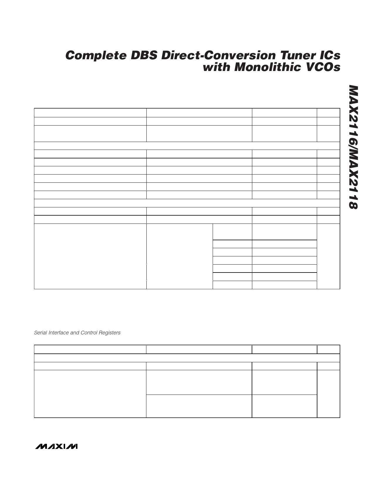
Complete DBS Direct-Conversion Tuner ICs
with Monolithic VCOs
DC ELECTRICAL CHARACTERISTICS (continued)
(VCC = +4.75V to +5.25V, GND = 0V, GC1 = +0.75V, no AC signal applied, default register settings, TA = 0°C to +85°C, unless other-
wise noted. Typical values are at VCC = +5V, TA = +25°C, unless otherwise noted.) (Note 1)
PARAMETER
Charge Pump Off-Leakage Current
Charge Pump Output Voltage Compliance
I2C INTERFACE—SDA, SCL
Clock Rate
Input Logic Level Low
Input Logic Level High
Input Hysteresis
Input Current
Output Logic Level Low
VTUNE ADC
Resolution
Input Voltage Range
ADC Reference Ladder Trip Point
CONDITIONS
MIN
-10
Charge-pump positive-to-negative current
matching of ±10%
0.4
TYP MAX UNITS
+10
nA
VCC -
0.6
V
6mA sink current
400
kHz
1.5
V
2.3
V
0.2
V
-10
+10
µA
0.6
V
(Note 4)
ADC read bits
110 to 111
101 to 110
100 to 101
011 to 100
010 to 011
001 to 010
000 to 001
3
Bits
0
VCC
V
VCC - VCC - VCC -
0.70 0.65 0.60
2.8 2.97 3.14
1.91 2.03 2.15
V
1.29 1.38 1.47
0.87 0.94 1.01
0.60 0.65 0.70
0.40 0.44 0.48
AC ELECTRICAL CHARACTERISTICS
(MAX2116/MAX2118 EV kits, VCC = +4.75V to +5.25V, GC1 and GC2 set for maximum gain, GND = 0V, IOUT = QOUT = 800mVP-P
(MAX2116), loaded with 1kΩ IOUT± = QOUT± = 590mVP-P differential (DL = 0, MAX2118), IOUT± = QOUT± = 1VP-P differential (DL
= 1, MAX2118), loaded with differential 2kΩ. Baseband LPF BW = 33MHz, fRFIN = 2175MHz. For default register values, see the
Serial Interface and Control Registers section. TA = +25°C to +85°C. Typical values are at VCC = +5V, TA = +25°C, unless otherwise
noted.) (Note 1)
PARAMETER
RF FRONT END
RF Input Frequency Range
Input Carrier Levels Necessary to Produce
800mVP-P at I/Q Baseband Outputs
(MAX2116)
CONDITIONS
TA = 0°C to +85°C
GC1 = 0.75V (max gain),
bits GC2(4) - GC2(0) = 00000 (max gain),
for output ≥ 800 mVP-P
GC1 = 2.6V (min gain),
bits GC2(4) - GC2(0) = 11111 (min gain),
for output ≤ 800mVP-P
MIN TYP MAX UNITS
925
2175 MHz
-77
-72
dBm
3
16
_______________________________________________________________________________________ 3
Share Link: 