MAX1697(1999) Ver la hoja de datos (PDF) - Maxim Integrated
Número de pieza
componentes Descripción
Fabricante
MAX1697 Datasheet PDF : 12 Pages
| |||
60mA, SOT23 Inverting Charge Pump
with Shutdown
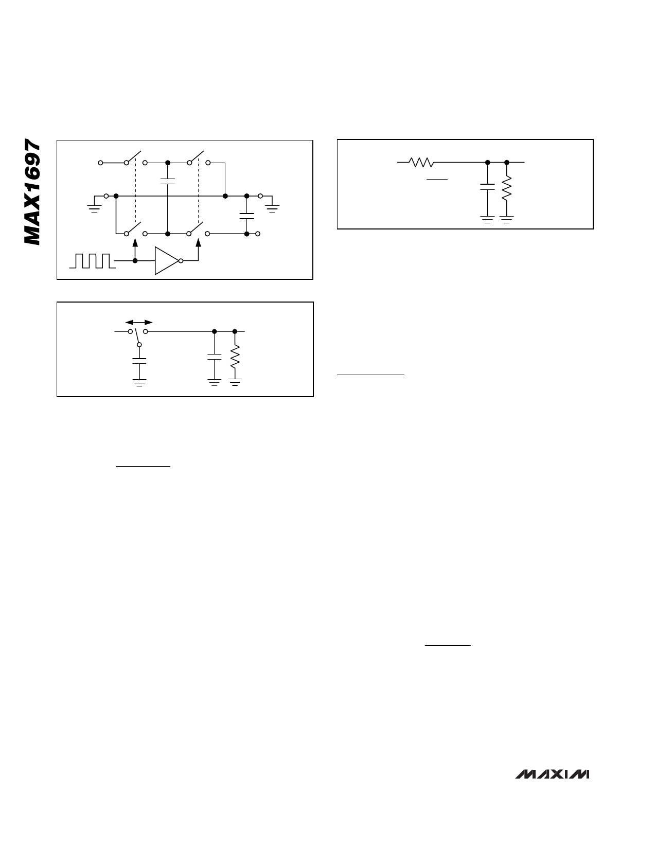
S1
S2
IN
C1
S3
S4
C2
VOUT = -(VIN)
REQUIV
V+
REQUIV
=
1
fOSC ·
C1
C2
Figure 3b. Equivalent Circuit
VOUT
RL
Figure 2. Ideal Voltage Inverter
fOSC
V+
C1
C2
VOUT
RL
Figure 3a. Switched-Capacitor Model
where the output impedance is roughly approximated
by:
( ) ROUT ≅
1
fOSC
⋅C1 + 2RSW
+ 4ESRC1 + ESRC2
The first term is the effective resistance of an ideal
switched-capacitor circuit (Figures 3a and 3b), and
RSW is the sum of the charge pump’s internal switch
resistances (typically 4Ω to 5Ω at VIN = +5V). The typi-
cal output impedance is more accurately determined
from the Typical Operating Characteristics.
Current Limit
The MAX1697 limits its input current upon start-up to
170mA (typ). This prevents low-current or higher output
impedance input supplies (such as alkaline cells) from
being overloaded when power is applied or when the
device awakes from shutdown.
Shutdown
The MAX1697 has a logic-controlled shutdown input.
Driving SHDN low places the device in a low-power
shutdown mode. The charge-pump switching halts,
supply current is reduced to 2nA, and OUT is actively
pulled to ground through a 3Ω resistance.
Driving SHDN high will restart the charge pump. The
switching frequency and capacitor values determine
how soon the device will reach 90% of the input voltage.
Thermal Shutdown
The MAX1697 has a thermal shutdown mode for addi-
tional protection against fault conditions. When the tem-
perature of the die exceeds +150°C, the internal clock
stops, suspending the device’s operation. The
MAX1697 resumes operation when the die temperature
falls 15°C. This prevents the device from rapidly oscil-
lating around the temperature trip point.
Applications Information
Capacitor Selection
The charge-pump output resistance is a function of the
ESR of C1 and C2. To maintain the lowest output resis-
tance, use capacitors with low ESR. (See Table 1 for a
list of recommended manufacturers.) Tables 2 and 3
suggest capacitor values for minimizing output resis-
tance or capacitor size.
Flying Capacitor (C1)
Increasing the flying capacitor’s value reduces the out-
put resistance. Above a certain point, increasing C1’s
capacitance has negligible effect because the output
resistance is then dominated by internal switch resis-
tance and capacitor ESR.
Output Capacitor (C2)
Increasing the output capacitor’s value reduces the
output ripple voltage. Decreasing its ESR reduces both
output resistance and ripple. Lower capacitance values
can be used with light loads if higher output ripple can
be tolerated. Use the following equation to calculate the
peak-to-peak ripple:
⋅ ⋅ VRIPPLE
=
IOUT
2(fOSC)C2
+
2
IOUT
ESRC2
Input Bypass Capacitor (C3)
If necessary, bypass the incoming supply to reduce its
AC impedance and the impact of the MAX1697’s switch-
ing noise. A bypass capacitor with a value equal to that
of C1 is recommended.
8 _______________________________________________________________________________________
Share Link: 