MAX1697(1999) Ver la hoja de datos (PDF) - Maxim Integrated
Número de pieza
componentes Descripción
Fabricante
MAX1697 Datasheet PDF : 12 Pages
| |||
60mA, SOT23 Inverting Charge Pump
with Shutdown
Typical Operating Characteristics (continued)
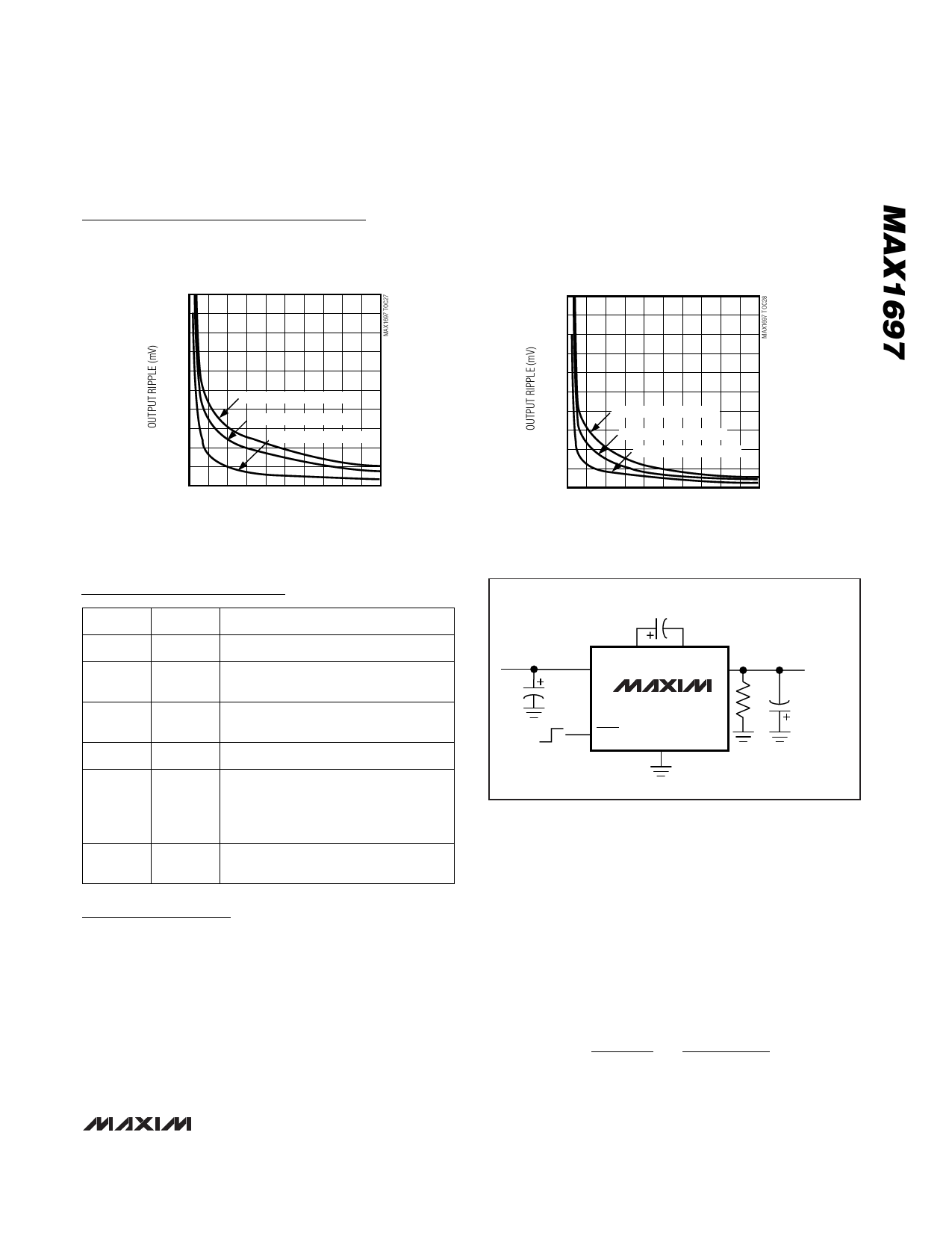
(Circuit of Figure 1, capacitors from Table 2, VIN = +5V, SHDN = IN, TA = +25°C, unless otherwise noted.)
MAX1697T
OUTPUT RIPPLE vs. CAPACITANCE
500
450
400
350
300
250
VIN = +4.75V, VOUT = -4.0V
200
VIN = +3.15V, VOUT = -2.5V
150
VIN = +1.9V, VOUT = -1.5V
100
50
0
0 1 2 3 4 5 6 7 8 9 10
CAPACITANCE (µF)
MAX1697U
OUTPUT RIPPLE vs. CAPACITANCE
500
450
400
350
300
250
200
VIN = +4.75V, VOUT = -4.0V
150
VIN = +3.15V, VOUT = -2.5V
100
VIN = +1.9V, VOUT = -1.5V
50
0
0 1 2 3 4 5 6 7 8 9 10
CAPACITANCE (µF)
Pin Description
PIN
NAME
FUNCTION
1
OUT
Inverting Charge-Pump Output
2
IN
Power-Supply Voltage Input. Input
range is 1.5V to 5.5V.
3
C1-
Negative Terminal of the Flying
Capacitor
4
GND Ground
Shutdown Input. Drive this pin high
5
SHDN
for normal operation; drive it low for
shutdown mode. OUT is actively
pulled to ground during shutdown.
6
C1+
Positive Terminal of the Flying
Capacitor
Detailed Description
The MAX1697 capacitive charge pumps invert the volt-
age applied to their input. For highest performance, use
low equivalent series resistance (ESR) capacitors (e.g.,
ceramic).
During the first half-cycle, switches S2 and S4 open,
switches S1 and S3 close, and capacitor C1 charges to
the voltage at IN (Figure 2). During the second half-
cycle, S1 and S3 open, S2 and S4 close, and C1 is level
shifted downward by VIN volts. This connects C1 in par-
allel with the reservoir capacitor C2. If the voltage across
C1
INPUT
1.5V to 5.5V
C3
ON
OFF
6
2
C1+
IN
3
C1-
1
OUT
MAX1697
RL
5 SHDN
GND
4
TE: (
Figure 1. Typical Application Circuit
NEGATIVE
OUTPUT
-1 · VIN
C2
C2 is smaller than the voltage across C1, charge flows
from C1 to C2 until the voltage across C2 reaches
-VIN. The actual voltage at the output is more positive
than -VIN, since switches S1–S4 have resistance and the
load drains charge from C2.
Efficiency Considerations
The efficiency of the MAX1697 is dominated by its qui-
escent supply current (IQ) at low output current and by
its output impedance (ROUT) at higher output current; it
is given by:
η
≅
IOUT
IOUT + IQ
1−
IOUT ⋅ROUT
VIN
_______________________________________________________________________________________ 7
Share Link: 