MAX1450 Ver la hoja de datos (PDF) - Maxim Integrated
Número de pieza
componentes Descripción
Fabricante
MAX1450 Datasheet PDF : 12 Pages
| |||
Low-Cost, 1%-Accurate Signal Conditioner
for Piezoresistive Sensors
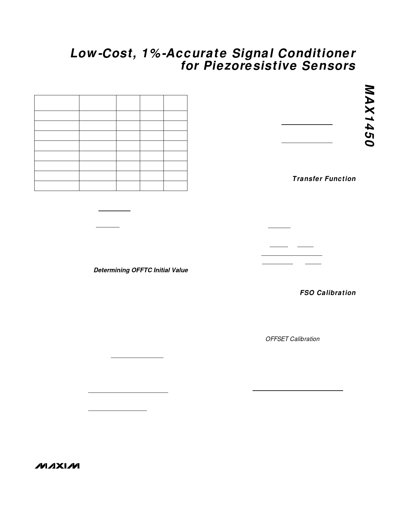
Table 3. PGA Gain Settings
PGA GAIN (V/V) PGA VALUE A2
A1
A0
39
0
0
0
0
65
1
0
0
1
91
2
0
1
0
117
3
0
1
1
143
4
1
0
0
169
5
1
0
1
195
6
1
1
0
221
7
1
1
1
A PGA
≈
OUTFSO
SensorFSO
≈ 4V = 106V/V
0.0375V
where OUTFSO is the desired calibrated transducer
full-span output voltage, and SensorFSO is the sensor
full-span output voltage at T1.
Determining OFFTC Initial Value
Generally, the OFFTC coefficient can be set to 0V,
since the offset TC errors will be compensated in a later
step. However, sensors with large offset TC errors may
require an initial coarse offset TC adjustment to prevent
the PGA from saturating as the temperature increases
during the compensation procedure. An initial coarse
offset TC adjustment would be required if the magni-
tude of the sensor offset TC error is more than about
10% of the FSO. If a coarse offset TC adjustment is
required, use the following equation:
OTC Correction =
∆VOUT(T)
∆VBDRIVE(T) x 1.15
which can be approximated by:
OTC Correction ≈
OTC x FSO x (∆T)
TCS x VBDRIVE x 1.15 x (∆T)
≈ −1030ppm / °C x 4V = 0.68
−2100 x 2.5V x 1.15
where OTC is the sensor offset TC error in ppm of FSO,
∆T is the operating temperature range in °C, and OTC
Correction is the offset TC resistor-divider ratio. For
positive values of OTC correction, connect SOTC to
VDD; for negative values, connect SOTC to VSS.
Select the Offset TC resistor divider (ROTCA and
ROTCB, Figure 4) using the following equation:
OTC Correction =
ROTCA
ROTCA + ROTCB
0.17 =
ROTCA
ROTCA + ROTCB
where 500kΩ ≥ (ROTCA + ROTCB) ≥ 100kΩ. Choose
ROTCB = 100kΩ and ROTCA = 20kΩ.
Transfer Function
The following transfer function (linearity correction not
included) is useful for data modeling or for developing
compensative algorithms:
VOUT = VBDRIVE x
VS x PGA + 1.15 x
VOFFTC
VDD
+
1.15 x
VOFFSET
where VBDRIVE =
VDD + VDD
RISRC RSTC
1
+1
AA x Rb(T) RSTC
(AA = current source gain)
FSO Calibration
Perform FSO calibration at room temperature with a full-
scale sensor excitation.
1) At +25°C (or T1), set VFSOTRIM to 2.5V. Adjust
RISRC until VBBUF = 2.5V.
2) Adjust VOFFSET until the room temperature offset
voltage is 0.5V (see OFFSET Calibration section).
3) Measure the full-span output (measuredVFSO).
4) Calculate VBIDEAL(25°C) using the following equation:
VBIDEAL(25o C) =
[ [ ] [ ] ] VFSOTRIM 1+
desiredVFSO − measuredVFSO
measuredVFSO
Note: If VBIDEAL(25°C) is outside the allowable bridge
voltage swing of (VSS + 1.3V) to (VDD - 1.3V), readjust
the PGA gain setting. If VBIDEAL(25°C) is too low,
decrease the PGA gain setting by one step and return
to Step 1. If VBIDEAL(25°C) is too high, increase the PGA
gain setting by one step and return to Step 1.
_______________________________________________________________________________________ 7
Share Link: 