M66515 Ver la hoja de datos (PDF) - Mitsumi
Número de pieza
componentes Descripción
Fabricante
M66515 Datasheet PDF : 7 Pages
| |||
MITSUBISHI 〈DIGITAL ASSP〉
M66515FP
LASER-DIODE DRIVER/CONTROLLER
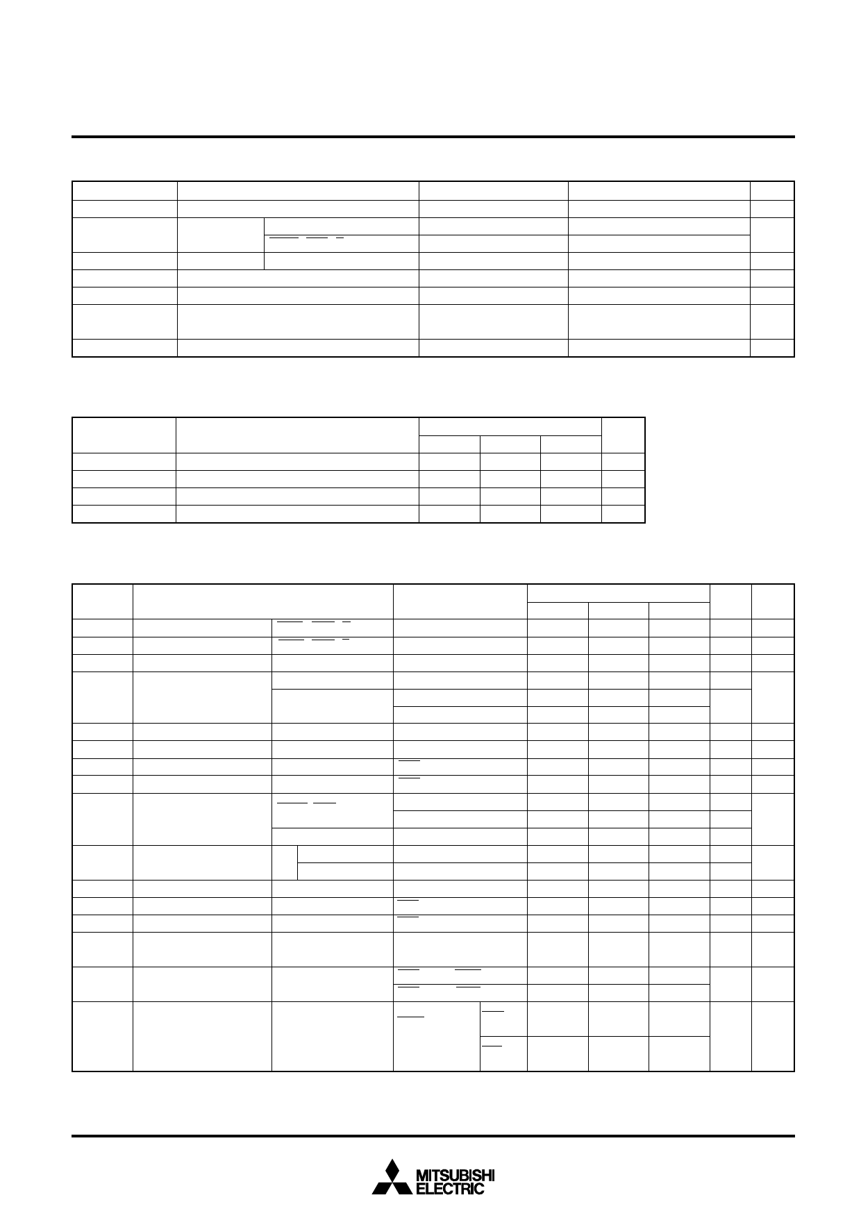
ABSOLUTE MAXIMUM RATINGS (Ta = –20 ~ 70°C unless otherwise noted)
Symbol
Parameter
Conditions
Ratings
Unit
VCC
Supply voltage
–0.5 ~ +7.0
V
CH, Vr
VI
Input voltage
DATE, ENB, S/H
–0.3 ~ VCC
V
–0.3 ~ +7.0
VO
Output voltage RO
–0.3 ~ +7.0
V
ISW
Switching current
150
mA
IB
Bias current
45
mA
Pd
Power dissipation
Measured being mounted
Ta = 25°C
1200
mW
Tstg
Storage temperature
–65 ~ 150
°C
RECOMMENDED OPERATIONAL CONDITIONS (Ta = –20 ~ 70°C unless otherwise noted)
Symbol
Parameter
Limits
Unit
Min.
Typ.
Max.
VCC
Supply voltage
4.75
5.0
5.25
V
ISW
Switing current
120
mA
IB
Bias current
30
mA
Topr
Operating ambient temperature
–20
70
°C
ELECTRICAL CHARACTERISTICS (Ta = –20 ~ 70°C, VCC = 5V±5% unless otherwise noted)
Symbol
VIH
VIL
Vr
Vref
VLD
VI
VOH
VOL
II
ISW
IB
Icg
Idg
Ioz
IOFF
ICC
Parameter
“H” Input voltage
DATA, ENB, S/H
Test conditions
Min.
2.0
“L” Input voltage
Reference voltage input
Reference voltage
output
Operating voltage range
Maximum effective voltage
“H” output voltage
“L” output voltage
Input current
Switching current (Note)
Bias current
(Note)
Load charging current
Load discharging current
DATA, ENB, S/H
Vr
Vref
Temprature
coefficient
LD
CH
CH
CH
DATA, ENB
CH
LD
Temprature coefficient
LD
CH
CH
IO = –10µA
Ta = –20 ~ 25°C
Ta = 20 ~ 70°C
ENB = 0.8V, IOH = –2mA
ENB = 0.8V, IOL = 2mA
VI = 2.7V
VI = 0.4V
VI = 0 ~ VCC
CH = 3.0V, RS = 300Ω, VLD = 2V
Ta = 20 ~ 70°C
VB = 1.2V, RB = 360Ω, VLD = 2V
ENB = 0.8V, VO = 0.6 ~ 4.0V
ENB = 0.8V, VO = 0.6 ~ 4.0V
0.4
2.5
VCC – 1.8
4.0
–0.66
0.66
Output current under off
condition
CH
VO = 0 ~ VCC, Hold condition
Output current under off
condition
LD
Supply current
ENB = 0.8V, DATA = 2.0V
ENB = 2.0V, DATA = 0.8V
VCC = 5.25V,
ENB = 0V,
DATA = 0V
CH = 3.0V, VB = 1.2V,
RS = 300Ω, RB = 360Ω, DATA = 4.5V
RO = LD = 5.0V
Limits
Typ.∗
1.2
–0.9
–0.9
VCC – 1.4
120
0.11
30
0.03
0.01
54
52
Max.
0.8
2.0
VCC
0.6
20
–0.2
±1
–2.0
2.0
±5
50
50
75
74
Unit
Test
circuit
V
V
V
V
1
mV/°C
V
V
V
1
V
1
µA
mA
µA
mA
2
mA/°C
mA
2
mA
3
mA
3
µA
3
µA
2
mA
4
∗ Typical values are gained under conditions of Ta = 25°C and Vcc = 5V.
Note: This parameter indicates the conversion characteristics of the input voltage and output current. In actual use, ISW and IB shall be within the range specified
as limits in the recommended operating conditions.
5
Share Link: 