M66515 Ver la hoja de datos (PDF) - Mitsumi
Número de pieza
componentes Descripción
Fabricante
M66515 Datasheet PDF : 7 Pages
| |||
MITSUBISHI 〈DIGITAL ASSP〉
M66515FP
LASER-DIODE DRIVER/CONTROLLER
FUNCTIONS
The M66515 is a semiconductor laser-diode driver/controller.
Its functions are the driving and laser power control of a spe-
cific type (Mitsubishi’s N type laser) of semiconductor laser
diode, in which the anode of a semiconductor laser diode
(LD) is connected in stem structure to the cathode of a moni-
toring photodiode (PD).
The functions to drive LD and to control laser power are car-
ried out by connecting an external capacitor to the CH pin and
applying a reference voltage to the Vr pin.
The PD current generated by LD illumination flows through
the resistor connected between 1RM and 2RM, thereby gen-
erating a potential difference (VM). VM is compared with the
voltage applied to the Vr pin. If VM < Vr, a constant current is
sourced through the CH pin so that the external capacitor is
charged. If VM > Vr, a constant current sinks through the CH
pin to discharge the external capacitor.
The above operation occurs when the S/H input is “L”
(sample). When the S/H input is “H,” the CH pin is maintained
at high impedance state (hold), irrespective of the state of VM,
Vr, and DATA input.
The LD drive current is made up of the switching current, ISW,
which is controlled by the DATA input, and IB, which is the
bias current to LD independent of the state of the DATA input.
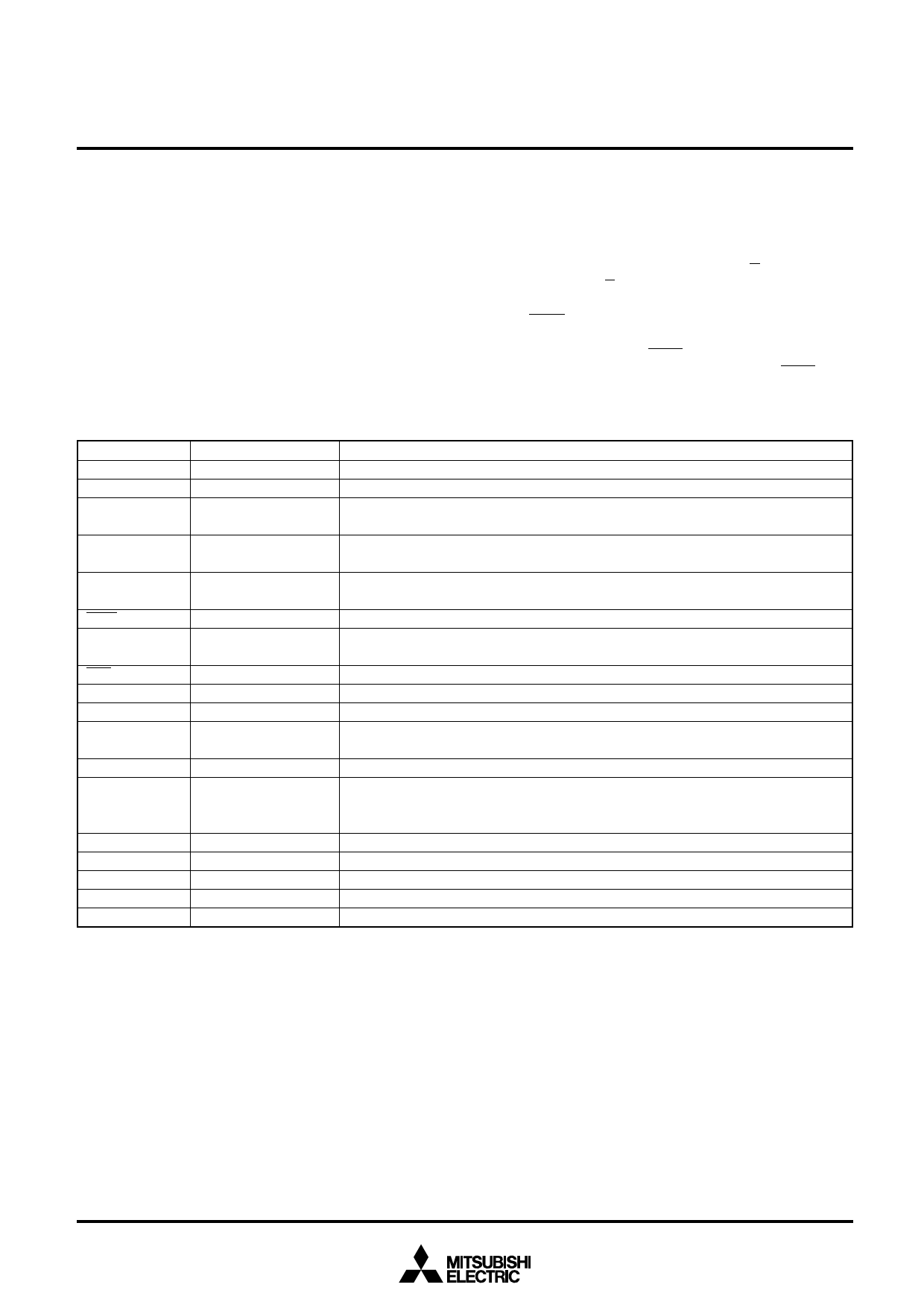
PIN DESCRIPTIONS
Pin
Name
LD
Laser current output
PD
Monitoring diode input
Switching current
RS
Set load output
Bias current
RB
Set load output
VB
Bias current setting
voltage input
Description
Connect to cathode on semiconductor laser diode.
Connect to anode on monitoring photodiode.
Connect a load resistor between this pin and GND for the setting of current (ISW) to be
switched.
Connect a load resistor between this pin and GND for the setting of bias current (IB). Leave
this pin open if IB is not used.
Bias current (IB) is set by applying a voltage at this pin. Leave this pin open if IB is not
used.
DATA
1RM, 2RM
ENB
RO
S/H
CH
Vref
Switching data input
For monitoring
Load input
Laser current enable input
If this pin is “L,” a current of ISW + IB flows through laser diode; if “H,” current IB flows.
A load resistor is connected between pins 1RM and 2RM for conversion of current
generated by monitoring photodiode into changes in voltage.
If this pin is “H” all current source circuits are turned off.
Laser current load output Connect a laser current load resistor between this pin and Vcc.
Sample hold control input If this pin is “L,” sampling (APC) occurs, if “H,” holding (switching).
Holding capacitor load
input/output
Connect a holding capacitor between this pin and GND. Inside the M66515 this pin
connects to the output of the sample-hold circuit and the current source input for ISW.
Reference voltage output Internal reference voltage (1.2 V typ.) output pin of M66515
A reference voltage is applied to this pin to operate the comparator in the sample-hold
Vr
Reference voltage input circuit. Connect this pin to the Vref pin if the internal reference voltage of the M66515 is to
be used.
TEST
VCC1
VCC2
GND1
GND2
Test pin
Power supply pin 1
Power supply pin 2
GND pin 1
GND pin 2
This pin is used to test the M66515 when shipped. Leave open.
Power supply to internal analog circuits. Connect to a positive power source (+5 V).
Power supply to internal digital circuits. connect to a positive power source (+5 V).
GND for internal analog circuits.
GND for internal digital circuits.
2
Share Link: 