M5M5V416BRT Ver la hoja de datos (PDF) - Renesas Electronics
Número de pieza
componentes Descripción
Fabricante
M5M5V416BRT Datasheet PDF : 10 Pages
| |||
revision-P11, ' 03.01.14
M5M5V416BTP,RT
MITSUBISHI LSIs
4194304-BIT (262144-WORD BY 16-BIT) CMOS STATIC RAM
DESCRIPTION
The M5M5V416B is a f amily of low v oltage 4-Mbit static RAMs
organized as 262,144-words by 16-bit, f abricated by Mitsubishi's
high-perf ormance 0.25µm CMOS technology .
The M5M5V416B is suitable f or memory applications where a
simple interf acing , battery operating and battery backup are the
important design objectiv es.
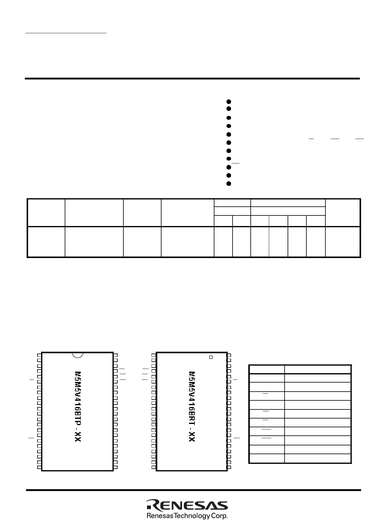
M5M5V416BTP,RT are packaged in a 44-pin 400mil thin small
outline package. M5M5V416BTP (normal lead bend ty pe package)
, M5M5V416BRT (rev erse lead bend ty pe package) , both ty pes
are v ery easy t o design a printed circuit board.
From the point of operating temperature, the f amily is div ided into
three v ersions; "Standard", "W-v ersion", and "I-v ersion". Those are
summarized in the part name table below.
Version,
Operating
temperature
Part name
Power
Supply
Access time
max.
I-v ersion
M5M5V416BTP,RT -70HI
-40 ~ +85°C
2.7 ~ 3.6V
70ns
FEATURES
Single +2.7~+3.6V power supply
Small stand-by current: 0.3µA(3V,ty p.)
No clocks, No ref resh
Data retention supply v oltage=2.0V to 3.6V
All inputs and outputs are TTL compatible.
Easy memory expansion by S1, S2, BC1 and BC2
Common Data I/O
Three-state outputs: OR-tie capability
OE prev ents data contention in the I/O bus
Process technology : 0.25µm CMOS
Package: 44 pin 400mil TSOP (II)
Stand-by c urrent Icc(PD), Vcc=3.0V
Activ e
ty pical *
Ratings (max.)
current
Icc1
25°C 40°C 25°C 40°C 70°C 85°C (3.0V, ty p.)
0.3µA 1µA 1µA 3µA 15µA 30µA
50mA
(10MHz)
7mA
(1MHz)
* "ty pical" parameter is sampled, not 100% tested.
PIN CONFIGURATION
A4 1
A3 2
A2 3
A1 4
A0 5
S1 6
DQ1 7
DQ2 8
DQ3 9
DQ4 10
Vcc 11
GND 12
DQ5 13
DQ6 14
DQ7 15
DQ8 16
WE 17
A15 18
A14 19
A13 20
A12 21
A16 22
44P3W-H
44
A5
43
A6
A5 44
A6 43
42
A7
41 OE
A7 42
OE 41
40
BC2
39
BC1
BC2 40
BC1 39
38
DQ16
DQ16
38
37
DQ15
DQ15
37
36
DQ14
DQ14
36
35
DQ13
DQ13
35
34 GND
GND
34
33
Vcc
Vcc
33
32
DQ12
DQ12
32
31
DQ11
DQ11
31
30
DQ10
DQ10
30
29
DQ9
DQ9
29
28
S2
S2 28
27
A8
A8
27
26
A9
A9 26
25
A10
24
A11
23
A17
A10 25
A11 24
A17 23
1
A4
2
A3
3
A2
4
A1
Pin
Function
5
A0
6
S1
A0 ~ A17 Address input
7 DQ1 DQ1 ~ DQ16 Data input / output
8
DQ2
9
DQ3
S1
Chip select input 1
10
DQ4
11
Vcc
12
GND
13
DQ5
14
DQ6
S2
Chip select input 2
W
Write control input
OE
Output enable input
15
DQ7
16
DQ8
17
WE
18
A15
19
A14
BC1
BC2
Vcc
Lower Byte (DQ1 ~ 8)
Upper Byte (DQ9 ~ 16)
Power supply
20
A13
21
A12
GND
Ground supply
22
A16
Outline: 44P3W-H/J
44P3W-J
NC: No Connection
1
Share Link: 