M5M5W816WG Ver la hoja de datos (PDF) - Renesas Electronics
Número de pieza
componentes Descripción
Fabricante
M5M5W816WG Datasheet PDF : 10 Pages
| |||
2002.04.18 Ver. 6.0
M5M5W816WG - 55HI, 70HI, 85HI
MITSUBISHI LSIs
8388608-BIT (524288-WORD BY 16-BIT) CMOS STATIC RAM
DESCRIPTION
FEATURES
The M5M5W816 is a f amily of low v oltage 8-Mbit static RAMs
organized as 524288-words by 16-bit, f abricated by Mitsubishi's
high-perf ormance 0.18µm CMOS technology .
The M5M5W816 is suitable f or memory applications where a
simple interf acing , battery operating and battery backup are the
important design objectiv es.
M5M5W816WG is packaged in a CSP (chip scale package),
with the outline of 7.5mm x 8.5mm, ball matrix of 6 x 8 (48ball)
and ball pitch of 0.75mm. It giv es the best solution f or a
compaction of m ounting area as well as f lexibility of wiring pattern
of printed circuit boards.
- Single 2.7~3.6V power supply
- Small stand-by current: 0.1µA (2V, ty p.)
- No clocks, No ref resh
- Data retention supply v oltage =2.0V
- All inputs and outputs are TTL compatible.
- Easy memory expansion by S1#, S2, BC1# and BC2#
- Common Data I/O
- Three-state outputs: OR-tie capability
- OE prev ents data contention in the I/O bus
- Process technology : 0.18µm CMOS
- Package: 48ball 7.5mm x 8.5mm CSP
Version,
Operating
temperature
I-version
-40 ~ +85°C
Part name
M5M5W816WG -55HI
M5M5W816WG -70HI
M5M5W816WG -85HI
Power
Supply
2.7 ~ 3.6V
Stand-by c urrent (µA)
Activ e
Access time
max.
* Ty pical(3.0V)
25°C 40°C
Ratings (max.@ Vcc=3.6V)
25°C 40°C 70°C 85°C
current
Icc1
*(3.0V, ty p.)
55ns
70ns
85ns
30mA
(10MHz)
0.5 1.0 5.0 8.0 20 40
5mA
(1MHz)
* Typical parameter indicates the value for the center
of distribution, and is not 100% tested.
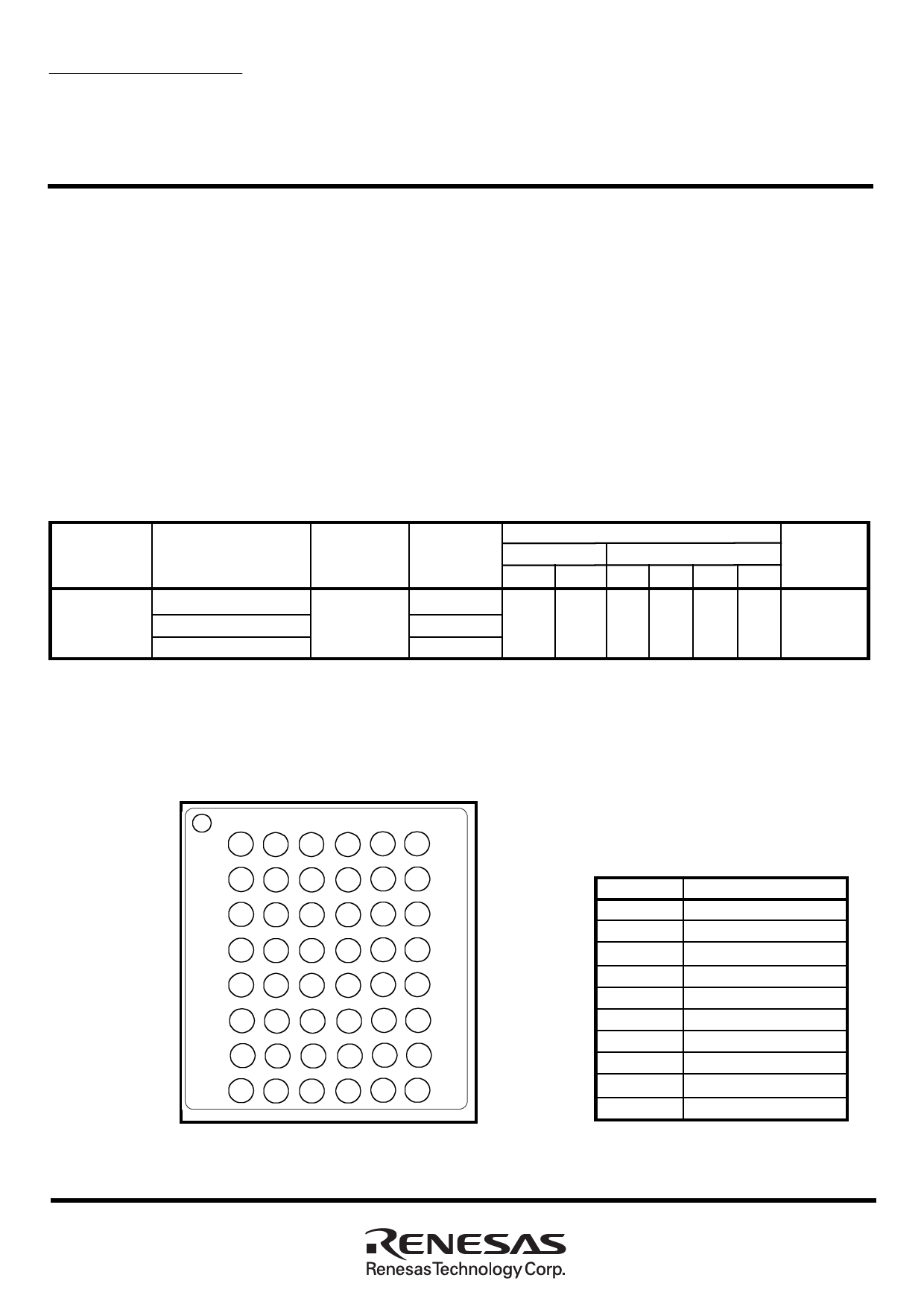
PIN CONFIGURATION
(TOP VIEW)
1 23 456
A BC1# OE#
A0
A1
A2
S2
B DQ16 BC2#
A3
A4
S1# DQ1
C DQ14 DQ15
A5
A6
DQ2 DQ3
D GND DQ13
A17
A7
DQ4
VCC
E VCC
DQ12
NC or
GND
A16
DQ5 GND
F DQ11 DQ10
A14
A15
DQ7 DQ6
G DQ9
N.C.
A12
A13
W#
DQ8
H A18
A8
A9
A10
A11
N.C.
Outline : 48F7Q
NC : No Connection
*Don't connect E3 ball to voltage level more than 0V.
Pin
Function
A0 ~ A18 Address input
DQ1 ~ DQ16 Data input / output
S1#
Chip select input 1
S2
Chip select input 2
W#
Write control input
OE# Output enable input
BC1# Lower By te (DQ1 ~ 8)
BC2# Upper By te (DQ9 ~ 16)
Vcc
Power supply
GND Ground supply
1
Share Link: 