M5M5V416BRT Ver la hoja de datos (PDF) - Mitsumi
Número de pieza
componentes Descripción
Fabricante
M5M5V416BRT Datasheet PDF : 11 Pages
| |||
revision-P04, ' 98.12.16
MITSUBISHI LSIs
M5M5V416BTP,RT
PRELIMINARY
Notice: This is not a final specification.
Some parametric limits are subject to change
AC ELECTRICAL CHARACTERISTICS
(1) TEST CONDITIONS
4194304-BIT (262144-WORD BY 16-BIT) CMOS STATIC RAM
(Vcc=2.7 ~ 3.6V, unless otherwise noted)
Supply v oltage
2.7V~3.6V
Input pulse
V IH= 2 . 4 V , V IL= 0 . 4 V
Input rise time and f all time 5ns
Ref erence lev el
Output loads
V OH=V OL= 1 . 5 V
Transition is measured ±500mV f rom
steady state voltage.(f or ten,t dis)
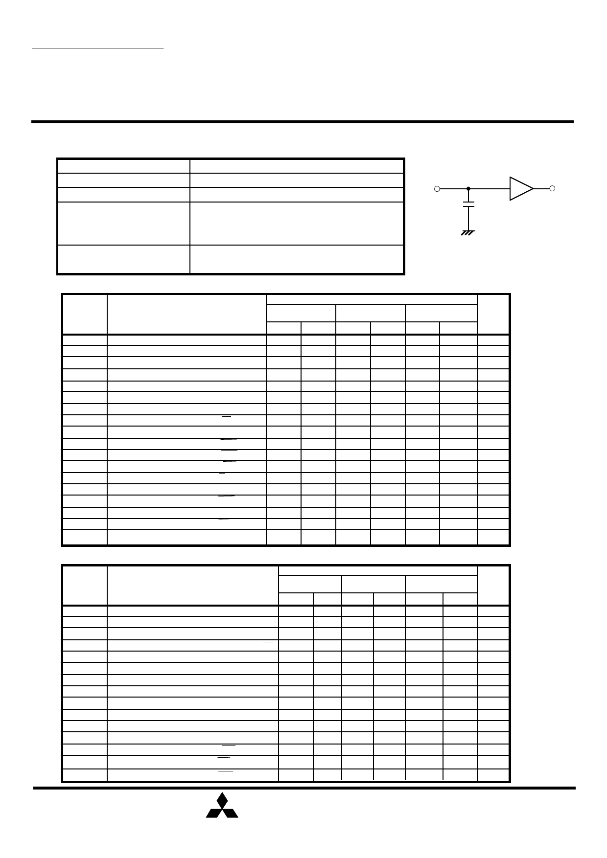
Fig.1,CL=30pF
CL=5pF (for ten,tdis)
1TTL
DQ
CL
Including scope and
jig capacitance
Fig.1 Output load
(2) READ CYCLE
Symbol
Parameter
t CR
ta(A)
ta(S1)
ta(S2)
ta(BC1)
ta(BC2)
ta(OE)
tdis(S1)
tdis(S2)
tdis(BC1)
tdis(BC2)
tdis(OE)
ten(S1)
ten(S2)
ten(BC1)
ten(BC2)
ten(OE)
tV(A)
Read cy cle time
Address access time
Chip select 1 access time
Chip select 2 access time
By te control 1 access time
By te control 2 access time
Output enable access time
Output disable time af t er S1 high
Output disable time af t er S2 low
Output disable time af t er BC1 high
Output disable time af t er BC2 high
Output disable time af t er OE high
Output enable time af ter S1 low
Output enable time af ter S2 high
Output enable time af ter BC1 low
Output enable time af ter BC2 low
Output enable time af ter OE low
Data v alid time after address
70L,70H,70LW
70HW,70LI,70HI
Min Max
70
70
70
70
70
70
35
25
25
25
25
25
10
10
10
10
10
Limits
85L,85H,85LW
85HW,85LI,85HI
Min Max
85
85
85
85
85
85
45
30
30
30
30
30
10
10
10
10
5
10
10L,10H,10LW
10HW,10LI,10HI Units
Min Max
100
ns
100 ns
100 ns
100 ns
100 ns
100 ns
50 ns
35 ns
35 ns
35 ns
35 ns
35 ns
10
ns
10
ns
10
ns
10
ns
5
ns
10
ns
(3) WRITE CYCLE
Symbol
Parameter
tCW
tw(W)
Write cy cle time
Write pulse width
tsu(A)
Address setup time
tsu(A-WH) Address setup time with respect to W
tsu(BC1) By te control 1 setup time
tsu(BC2) By te control 2 setup time
tsu(S1) Chip select 1 setup time
tsu(S2) Chip select 2 setup time
tsu(D)
Data setup time
th(D)
Data hold time
trec(W) Write recov ery time
tdis(W) Output disable time f rom W low
tdis(OE) Output disable time f rom OE high
ten(W) Output enable time f rom W high
ten(OE) Output enable time f rom OE low
Limits
70L,70H,70LW 85L,85H,85LW
70HW,70LI,70HI 85HW,85LI,85HI
Min Max Min Max
70
85
55
60
0
0
65
70
65
70
65
70
65
70
65
70
35
35
0
0
0
0
25
30
25
30
5
5
5
5
10L,10H,10LW
10HW,10LI,10HI
Min Max
100
75
0
85
85
85
85
85
40
0
0
35
35
5
5
Units
ns
ns
ns
ns
ns
ns
ns
ns
ns
ns
ns
ns
ns
ns
ns
MITSUBISHI ELECTRIC
4
Share Link: 