AD1376 Ver la hoja de datos (PDF) - Analog Devices
Número de pieza
componentes Descripción
Fabricante
AD1376 Datasheet PDF : 8 Pages
| |||
AD1376/AD1377
Return pin and the logic supply is bypassed to the Logic Power
Return pin.
The metal cover is internally grounded with respect to the
power supplies, grounds and electrical signals. Do not externally
ground the cover.
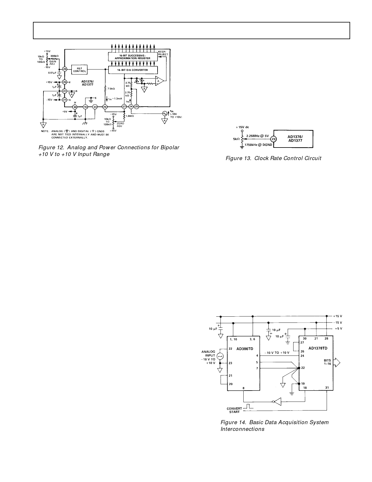
CLOCK RATE CONTROL
The AD1376/AD1377 may be operated at faster conversion
times by connecting the Clock Rate Control (Pin 23) to an
external multiturn trim potentiometer (TCR <100 ppm/°C) as
shown in Figure 13.
Figure 12. Analog and Power Connections for Bipolar
+10 V to +10 V Input Range
Other Ranges
Representative digital coding for 0 V to +10 V and –10 V to
+10 V ranges is given above. Coding relationships and calibra-
tion points for 0 V to +5 V, –2.5 V to +2.5 V and –5 V to +5 V
ranges can be found by halving proportionally the corresponding
code equivalents listed for the 0 V to +10 V and –10 V to +10 V
ranges, respectively, as indicated in Table III.
Zero and full-scale calibration can be accomplished to a preci-
sion of approximately ± 1/2 LSB using the static adjustment
procedure described above. By summing a small sine or triangu-
lar wave voltage with the signal applied to the analog input, the
output can be cycled through each of the calibration codes of
interest to more accurately determine the center (or end points)
of each discrete quantization level. A detailed description of this
dynamic calibration technique is presented in Analog-Digital
Conversion Handbook, edited by D. H. Sheingold, Prentice Hall,
Inc., 1986.
GROUNDING, DECOUPLING AND LAYOUT
CONSIDERATIONS
Many data-acquisition components have two or more ground
pins which are not connected together within the device. These
“grounds” are usually referred to as the Logic Power Return,
Analog Common (Analog Power Return) and Analog Signal
Ground. These grounds (Pins 19 and 22) must be tied together
at one point for the ADC as close as possible to the converter.
Ideally, a single solid analog ground plane under the converter
would be desirable. Current flows through the wires and etch
stripes of the circuit cards, and since these paths have resistance
and inductance, hundreds of millivolts can be generated be-
tween the system analog ground point and the ground pins of
the ADC. Separate wide conductor stripe ground returns should
be provided for high resolution converters to minimize noise
and IR losses from the current flow in the path from the con-
verter to the system ground point. In this way ADC supply
currents and other digital logic-gate return currents are not
summed into the same return path as analog signals where they
would cause measurement errors.
Each of the ADC supply terminals should be capacitively de-
coupled as close to the ADC as possible. A large value capacitor
such as 1 µF in parallel with a 0.1 µF capacitor is usually suffi-
cient. Analog supplies are to be bypassed to the Analog Power
Figure 13. Clock Rate Control Circuit
HIGH RESOLUTION DATA ACQUISITION SYSTEM
The essential details of a high resolution data acquisition system
using the AD386 and AD1376 or AD1377 are shown in Figure
14. Conversion is initiated by the falling edge of the CONVERT
START pulse. This edge drives the AD1376’s or AD1377’s
STATUS line high. The inverter then drives the AD386 into
hold mode. STATUS remains high throughout the conversion
and returns low once the conversion is completed. This allows
the AD386 to reenter track mode.
This circuit can exhibit nonlinearities arising from transients
produced at the A/D’s input by the falling edge of CONVERT
START. This edge resets the A/D’s internal DAC; the resulting
transient depends on the SHA’s present output voltage and the
A/D’s prior conversion result. In the circuit of Figure 14 the
falling edge of CONVERT START also places the SHA into
hold mode (via the A/D’s STATUS output), causing the reset
transient to occur at the same moment as the SHA’s track-and-
hold transition. Timing skews and capacitive coupling can cause
some of the transient signal to add to the signal being acquired
by the SHA, introducing nonlinearity.
Figure 14. Basic Data Acquisition System
Interconnections
A much safer approach is to add a flip flop as shown in Figure
15. The rising edge of CONVERT START places the T/H into
hold mode before the A/D reset transients begin. The falling
REV. B
–7–
Share Link: 