AD1377JD(RevD) Ver la hoja de datos (PDF) - Analog Devices
Número de pieza
componentes Descripción
Fabricante
AD1377JD Datasheet PDF : 12 Pages
| |||
AD1376/AD1377
DESCRIPTION OF OPERATION
AD1376/AD1377KD
0.0135
±2ppm/°C,
±0.003%, @ 25°C
AD1376/AD1377JD
±3ppm/°C,
±0.006%, @ 25°C
0.0080
0.0060
0.0030
0
–0.0030
–0.0060
–0.0080
–0.0135
0
25
TEMPERATURE (°C)
Figure 2. Linearity Error vs. Temperature
AD1376
0.0195
0.0120
0
–0.0120
–0.0195
70
0.100
0.010
SHORT CYCLED TO 12 BITS
SHORT CYCLED TO 13 BITS
SHORT CYCLED TO 14 BITS
1/2LSB 12-BIT
0.006
0.003
0.001
5
1/2LSB 13-BIT
1/2LSB 14-BIT
10
15
20
CONVERSION TIME (µs)
Figure 3. AD1376 Nonlinearity vs. Conversion Time
0.100
0.038
0
–0.038
–0.100
0.068
0
–0.068
0
10
20
30
40
50
60
70
Figure 4. Gain Drift Error vs. Temperature
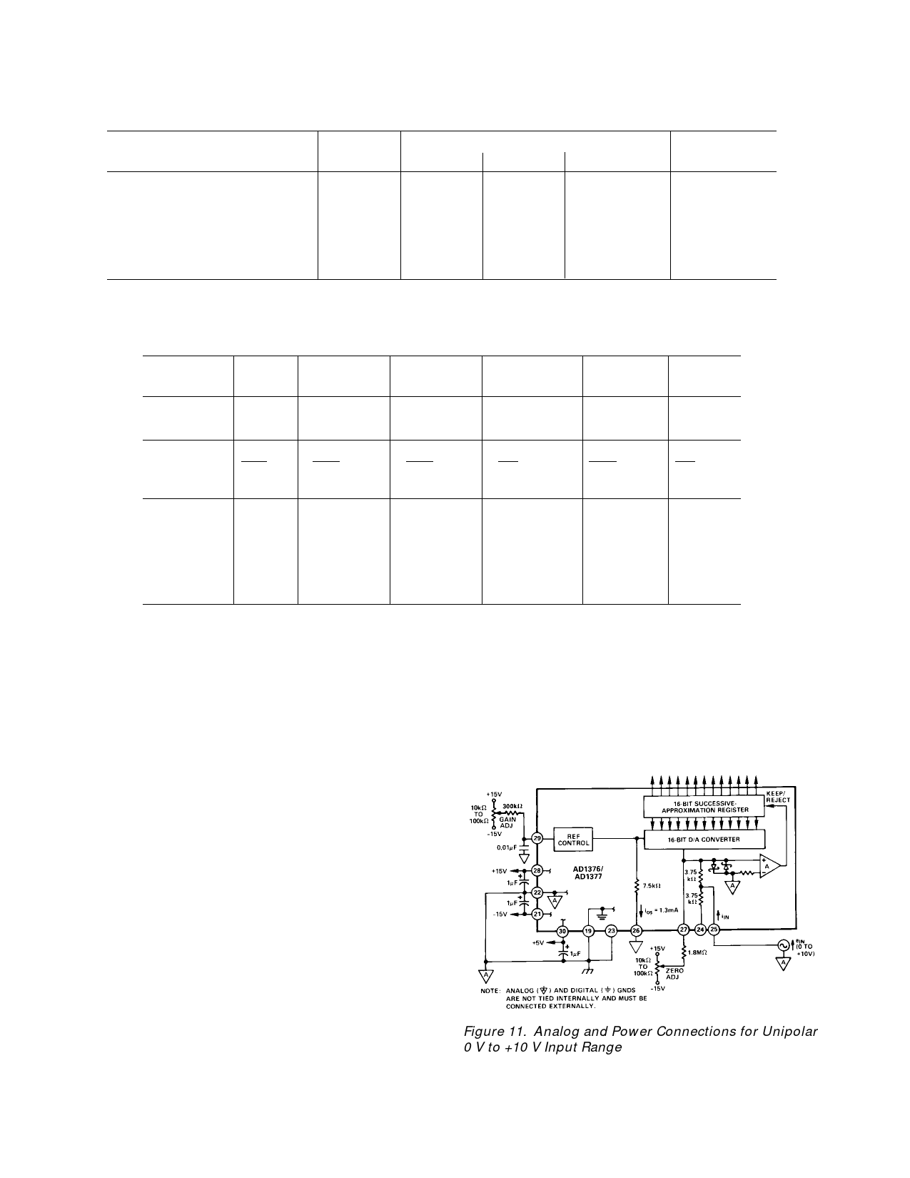
On receipt of a CONVERT START command, the AD1376/
AD1377 convert the voltage at the analog input into an
equivalent 16-bit binary number. This conversion is
accomplished as follows: the 16-bit successive approximation
register (SAR) has its 16-bit outputs connected both to the
device bit output pins and to the corresponding bit inputs of the
feedback DAC. The analog input is successively compared to
the feedback DAC output, one hit at a time (MSB first, LSB
last). The decision to keep or reject each bit is then made at the
completion of each bit comparison period, depending on the
state of the comparator at that time.
GAIN ADJUSTMENT
The gain adjustment circuit consists of a 100 ppm/°C poten-
tiometer connected across ±VS with its slider connected
through a 300 kΩ resistor to Pin 29 (GAIN ADJ) as shown in
Figure 5.
If no external trim adjustment is desired, Pin 27
(COMPARATOR IN) and Pin 29 can be left open.
+15V
10kΩ
100ppm/°C TO
100kΩ
300kΩ
0.01µF
–15V
29 AD1376/AD1377
Figure 5. Gain Adjustment Circuit (±0.2% FSR)
ZERO OFFSET ADJUSTMENT
The zero offset adjustment circuit consists of a 100 ppm/°C
potentiometer connected across ±VS with its slider connected
through a 1.8 MΩ resistor to Pin 27 for all ranges. As shown in
Figure 6, the tolerance of this fixed resistor is not critical; a carbon
composition type is generally adequate. Using a carbon compo-
sition resistor having a −1200 ppm/°C temperature coefficient
contributes a worst-case offset temperature coefficient of 32 LSB14
× 61 ppm/LSB14 × 1200 ppm/°C = 2.3 ppm/°C of FSR, if the offset
adjustment potentiometer is set at either end of its adjustment
range. Since the maximum offset adjustment required is typically
no more than ±16 LSB14, use of a carbon composition offset
summing resistor typically contributes no more than 1 ppm/°C of
FSR offset temperature coefficient.
+15V
10kΩ
TO
100kΩ
1.8MΩ
27 AD1376/AD1377
–15V
Figure 6. Zero Offset Adjustment Circuit (±0.3% FSR)
An alternate offset adjustment circuit, which contributes a
negligible offset temperature coefficient if metal film resistors
(temperature coefficient <100 ppm/°C) are used, is shown in
Figure 7.
+15V
OFFSET
ADJ
10kΩ
TO
100kΩ
180kΩ M.F. 180kΩ M.F.
27 AD1376/AD1377
22kΩ M.F.
–15V
Figure 7. Low Temperature Coefficient Zero Adjustment Circuit
Rev. D | Page 6 of 12
Share Link: 