M59DR032EA Ver la hoja de datos (PDF) - STMicroelectronics
Número de pieza
componentes Descripción
Fabricante
M59DR032EA Datasheet PDF : 43 Pages
| |||
M59DR032EA, M59DR032EB
BUS OPERATIONS
The following operations can be performed using
the appropriate bus cycles: Read Array (Random,
and Page Modes), Write, Output Disable, Standby
and Reset/Power-Down, see Table 3.
Read. Read operations are used to output the
contents of the Memory Array, the Electronic Sig-
nature, the Status Register, the CFI, the Block
Protection Status or the Configuration Register
status. Read operation of the memory array is per-
formed in asynchronous page mode, that provides
fast access time. Data is internally read and stored
in a page buffer. The page has a size of 4 words
and is addressed by A0-A1 address inputs. Read
operations of the Electronic Signature, the Status
Register, the CFI, the Block Protection Status, the
Configuration Register status and the Security
Code are performed as single asynchronous read
cycles (Random Read). Both Chip Enable E and
Output Enable G must be at VIL in order to read the
output of the memory.
Write. Write operations are used to give com-
mands to the memory or to latch Input Data to be
programmed. A write operation is initiated when
Chip Enable E and Write Enable W are at VIL with
Output Enable G at VIH. Addresses are latched on
the falling edge of W or E whichever occurs last.
Commands and Input Data are latched on the ris-
ing edge of W or E whichever occurs first. Noise
pulses of less than 5ns typical on E, W and G sig-
nals do not start a write cycle.
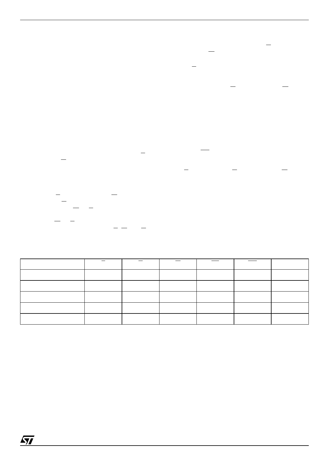
Table 3. Bus Operations
Operation
E
G
Read
VIL
VIL
Write
VIL
VIH
Output Disable
VIL
VIH
Standby
VIH
X
Reset / Power-Down
X
X
Note: X = Don’t care.
Output Disable. The data outputs are high im-
pedance when the Output Enable G is at VIH with
Write Enable W at VIH.
Standby. The memory is in standby when Chip
Enable E is at VIH and the P/E.C. is idle. The pow-
er consumption is reduced to the standby level
and the outputs are high impedance, independent
of the Output Enable G or Write Enable W inputs.
Automatic Standby. In Read mode, after 150ns
of bus inactivity and when CMOS levels are driving
the addresses, the chip automatically enters a
pseudo-standby mode where consumption is re-
duced to the CMOS standby value, while outputs
still drive the bus.
Power-Down. The memory is in Power-Down
when the Configuration Register is set for Power-
Down and RP is at VIL. The power consumption is
reduced to the Power-Down level, and Outputs are
in high impedance, independent of the Chip En-
able E, Output Enable G or Write Enable W inputs.
Dual Bank Operations. The Dual Bank allows
data to be read from one bank of memory while a
program or erase operation is in progress in the
other bank of the memory. Read and Write cycles
can be initiated for simultaneous operations in dif-
ferent banks without any delay. Status Register
during Program or Erase must be monitored using
an address within the bank being modified.
W
RP
WP
DQ15-DQ0
VIH
VIH
VIH
Data Output
VIL
VIH
VIH
Data Input
VIH
VIH
VIH
Hi-Z
X
VIH
VIH
Hi-Z
X
VIL
VIH
Hi-Z
9/43
Share Link: 