M58LW064 Ver la hoja de datos (PDF) - STMicroelectronics
Número de pieza
componentes Descripción
Fabricante
M58LW064 Datasheet PDF : 53 Pages
| |||
M58LW064A, M58LW064B
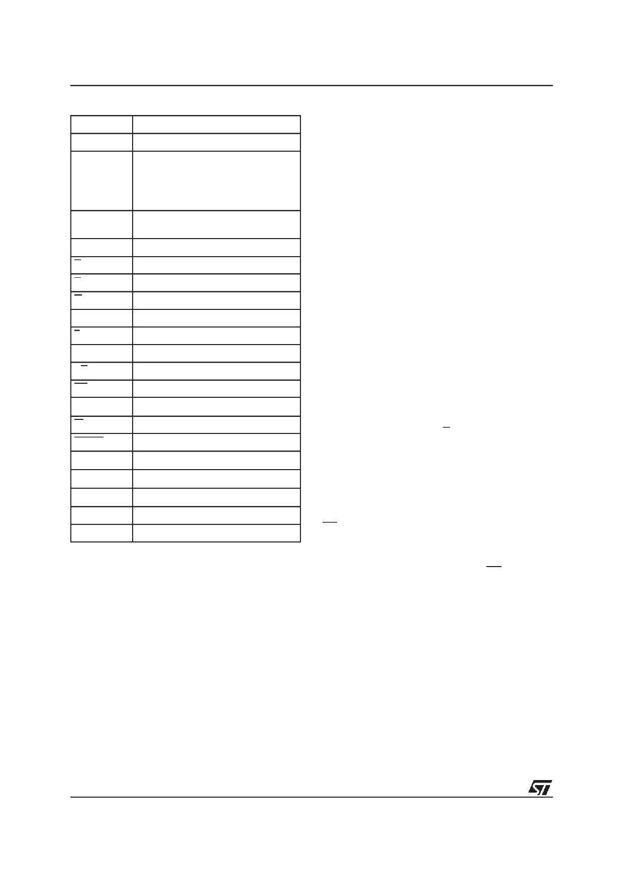
Table 1. Signal Names
A1-A22
Address Inputs x16 Organisation
A2-A22
Address inputs x32 Organisation
DQ0-DQ7
Data Input/Output x16 and x32
Organisation Command Input,
Electronic Signature Output, Block
Protection Ststus Output, Status
Register Output
DQ8-DQ15
Data Input/Output x16 and x32
Organisation
DQ16-DQ31 Data Input/Output x32 Organisation
B
Burst Address Advance
E
Chip Enable
G
Output Enable
K
Burst Clock
L
Latch Enable
R
Valid Data Ready (open drain output)
RB
Ready/Busy (open drain output)
RP
Reset/Power-down
VPP
Program/Erase Enable
W
Write Enable
WORD
Word Organisation (M58LW064B only)
VDD
Supply Voltage
VDDQ
Input/Output Supply Voltage
VSS
Ground
NC
No internal connection
DU
Don’t Use (internally connected)
The devices support Asynchronous Random and
Latch Enable Controlled Read with Page mode as
well as Synchronous Burst Read with a config-
urable burst. They also support pipelined synchro-
nous Burst Read. Writing is Asynchronous or
Asynchronous Latch Enable Controlled.
The configurable synchronous burst read interface
allows a high data transfer rate controlled by the
Burst Clock K signal. It is capable of bursting fixed
or unlimited lengths of data. The burst type, laten-
cy and length are configurable and can be easily
adapted to a large variety of system clock frequen-
cies and microprocessors. A 16 Word or 8 Double-
Word Write Buffer improves effective program-
ming speed by up to 20 times when data is pro-
grammed in full buffer increments. Effective Word
programming takes typically 12µs. The array ma-
trix organisation allows each block to be erased
and reprogrammed without affecting other blocks.
Program and Erase operations can be suspended
in order to perform either Read or Program in any
other block and then resumed. All blocks are pro-
tected against spurious programming and erase
cycles at power-up. Any block can be separately
protected at any time. The block protection bits
can also be deleted, this is executed as one se-
quence for all blocks simultaneously. Block protec-
tion can be temporarily disabled. Each block can
be programmed and erased over 100,000 cycles.
Block erase is performed in typically 1 second.
An internal Command Interface (C.I.) decodes In-
structions to access/modify the memory content.
The Program/Erase Controller (P/E.C.) automati-
cally executes the algorithms taking care of the
timings required by the program and erase opera-
tions. Verification is internally performed and a
Status Register tracks the status of the operations.
The Ready/Busy output RB indicates the comple-
tion of operations.
Instructions are written to the memory through the
Command Interface (C.I.) using standard micro-
processor write timings. The device supports the
Common Flash Interface (CFI) command set defi-
nition.
A Reset/Power-down mode is entered when the
RP input is Low. In this mode the power consump-
tion is lower than in the normal standby mode, the
device is write protected and both the Status and
the Burst Configuration Registers are cleared. A
recovery time is required when the RP input goes
High.
The device is offered in various package versions,
TSOP56 (14 x 20 mm), TSOP86 Type II (11.76 x
22.22 mm) and LBGA54 1mm ball pitch for the
M58LW064A and PQFP80 for the M58LW064B.
2/53
Share Link: 