M5481 Ver la hoja de datos (PDF) - STMicroelectronics
Número de pieza
componentes Descripción
Fabricante
M5481 Datasheet PDF : 10 Pages
| |||
M5481
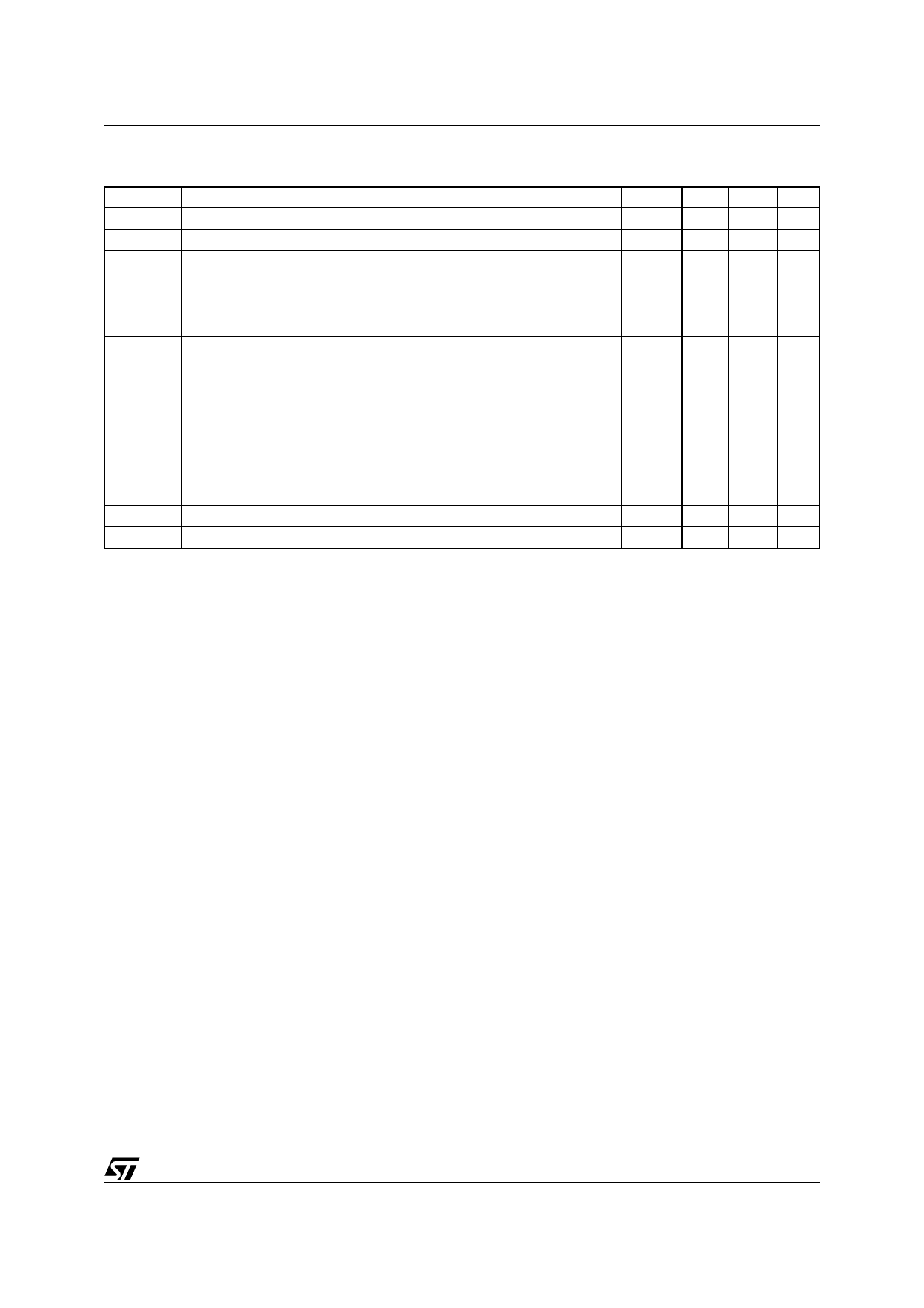
Table 2. Static Electrical Characteristics
(Tamb within operating range, VDD = 4.75V to 13.2V, VSS = 0V, unless otherwise specified)
Symbol
Parameter
Test Conditions
Min. Typ. Max.
VDD Supply Voltage
4.5
13.2
IDD
Supply Current
VDD = 13.2V
7
VI
Input Voltage Logical "0" Level ± 10µA Input Bias
Logical "1" Level
4.75 ≤ VDD ≤ 5.25
- 0.3
0.8
2.2
VDD
VDD > 5.25
VDD - 2
VDD
IB
Brightness Input Current (note 2)
0
0.75
VB
Brightness Input Voltage (pin 9) Input Current = 750µA, Tamb = 25°C 3
4.3
VO(off) Off State Out. Voltage
13.2
IO
Out. Sink Current (note 3)
Segment OFF
VO = 3V
10
Segment ON
VO = 1V (note 4)
Brightness In. = 0µA
0
10
Brightness In. = 100µA
2
2,7
4
Brightness In. = 750µA
12
15 25
fclock Input Clock Frequency
0
0.5
IO
Output Matching (note 1)
± 20
Note: 1. Output matching is calculated as the percent variation from I MAX + IMIN/2.
2. With a fixed resistor on the brightness input some variation in brightness will occur from one device to another.
3. Absolute maximum for each output should be limited to 40mA.
4. The VO voltage should be regulated by the user.
Unit
V
mA
V
V
V
mA
V
V
µA
µA
mA
mA
MHz
%
FUNCTIONAL DESCRIPTION
The M5481 uses the M5450 die which is packaged
to operate 2-digit alphanumeric displays with min-
imal interface with the display and the data source.
Serial data transfer from the data source to the dis-
play driver is accomplished with 2 signals, serial
data and clock. using a format of a leading “1” fol-
lowed by the 35 data bits allows data transfer with-
out an additional load signal.
The 35 data bits are latched after the 36th bit is
complete, thus providing non-multiplexed, direct
drive to the display. Outputs change only if the se-
rial data bits differ from the previous time. Display
brightness is determined by control of the output
current for LED displays. A 1nF capacitor should
be connected to brightness control (pin 9) to pre-
vent possible oscillations.
A block diagram is shown on Figure 3. The output
current is typically 20 times greater than the cur-
rent into pin 9, which is set by an external variable
resistor.
The latter is an internal limiting resistor of 400Ω
nominal value.
Figure 4 shows the input data format. A start bit of
logical “1” precedes the 35 bits of data. At the 36th
clock a LOAD is generated synchronously with the
high state of the clock, which loads the 35 bits of
the shift registers into the latches.
3/10
Share Link: 