M37906F8CFP Ver la hoja de datos (PDF) - Renesas Electronics
Número de pieza
componentes Descripción
Fabricante
M37906F8CFP Datasheet PDF : 35 Pages
| |||
PRELIMINARY NSootimcee: pTahriasmisentroict alimfinitsalasrpeescuifbicjeactitotno. change.
MITSUBISHI MICROCOMPUTERS
M37906F8CFP, M37906F8CSP
16-BIT CMOS MICROCOMPUTER
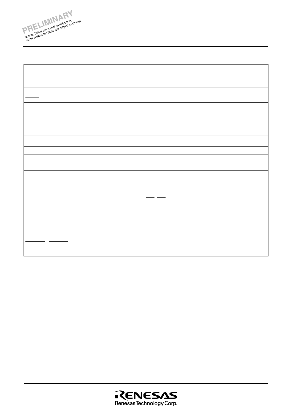
PIN DESCRIPTION (MICROCOMPUTER MODE)
Pin
Name
Input/
Output
Functions
Vcc, Vss Power supply input
— Apply 5 V±0.5 V to Vcc, and 0 V to Vss.
MD0
MD0
Input Connect this pin to VSS.
MD1
MD1
Input Connect this pin to Vss.
RESET
Reset input
Input The microcomputer is reset when “L” level is applied to this pin.
XIN
XOUT
Clock input
Clock output
Input
Output
These are input and output pins of the internal clock generating circuit. Connect a
ceramic or quartz-crystal oscillator between the XIN and XOUT pins. When an
external clock is used, the clock source should be connected to the XIN pin, and the
XOUT pin should be left open.
VCONT
Filter circuit connection
— When using the PLL frequency multiplier, connect this pin to the filter circuit. When
not using the PLL frequency multiplier, this pin should be left open.
AVcc,
AVss
Analog power supply input
— Power supply input pins for the A-D converter and the D-A converter. Connect AVcc
to Vcc, and AVss to Vss externally.
VREF
Reference voltage input
Input This is the reference voltage input pin for the A-D converter and the D-A converter.
P10–P17 I/O port P1
I/O Port P1 is an 8-bit I/O port. This port has an I/O direction register, and each pin
can be programmed for input or output. These pins enter the input mode
at reset. These pins also function as I/O port pins of UART0 and UART1.
P20–P27 I/O port P2
I/O In addition to having the same functions as port P1, these pins also function as I/O
pins for timers A4 and A9. By software setting, these pins also function as input
pins for timers B0–B2, an input pin for INT3, and a trigger input pin in the pulse
output port mode.
P50–P57 I/O port P5
I/O In addition to having the same functions as port P1, these pins also function as
input pins for INT5–INT7, input pins for timers B0–B2, and input pins for position-
data-input pins in the three-phase waveform mode.
P60–P65 I/O port P6
I/O In addition to having the same functions as port P1, these pins also function as I/O
pins for timers A0–A2, and output pins for the motor drive waveform.
P70–P74 I/O port P7
I/O In addition to having the same functions as port P1, these pins also function as
input pins for the A-D converter. P73 functions as an output pin for the D-A
converter; P74 functions as an output pin for the D-A converter, an input pin for
INT3, and a trigger input pin in the pulse output port mode.
P6OUTCUT P6OUTCUT input
Input
This pin has the function to forcibly place port P6 pins in the input mode. Also, this
pin functions as an input pin for INT4; and this pin is used to input a signal, which
forcibly cuts off a motor drive waveform output.
7
Share Link: 