M37735S4LHP Ver la hoja de datos (PDF) - Renesas Electronics
Número de pieza
componentes Descripción
Fabricante
M37735S4LHP Datasheet PDF : 37 Pages
| |||
New product
MITSUBISHI MICROCOMPUTERS
M37735S4LHP
16-BIT CMOS MICROCOMPUTER
PROCESSOR MODE
Only the microprocessor mode can be selected.
___
Figure 9 shows the functions of pins P00/CS0 — P47 in the
microprocessor mode.
Figure 10 shows external memory area for the microprocessor mode.
Access to the external memory is affected by the BYTE pin, the wait
bit (bit 2 of the processor mode register 0 at address 5E16), and the
wait selection bit (bit 0 of the processor mode register 1 at address
5F16) .
• BYTE pin
When accessing the external memory, the level of the BYTE pin is
used to determine whether to use the data bus as 8-bit width or 16-
bit width.
The data bus has a width of 8 bits when level of the BYTE pin is “H”,
and pins P20/A0/D0 — P27/A7/D7 are the data I/O pins.
The data bus has a width of 16 bits when the level of the BYTE pin is
“L”, and pins P20/A0/D0 — P27/A7/D7 and pins P10/A8/D8 — P17/A15/
D15 are the data I/O pins.
When accessing the internal memory, the data bus always has a
width of 16 bits regardless of the BYTE pin level.
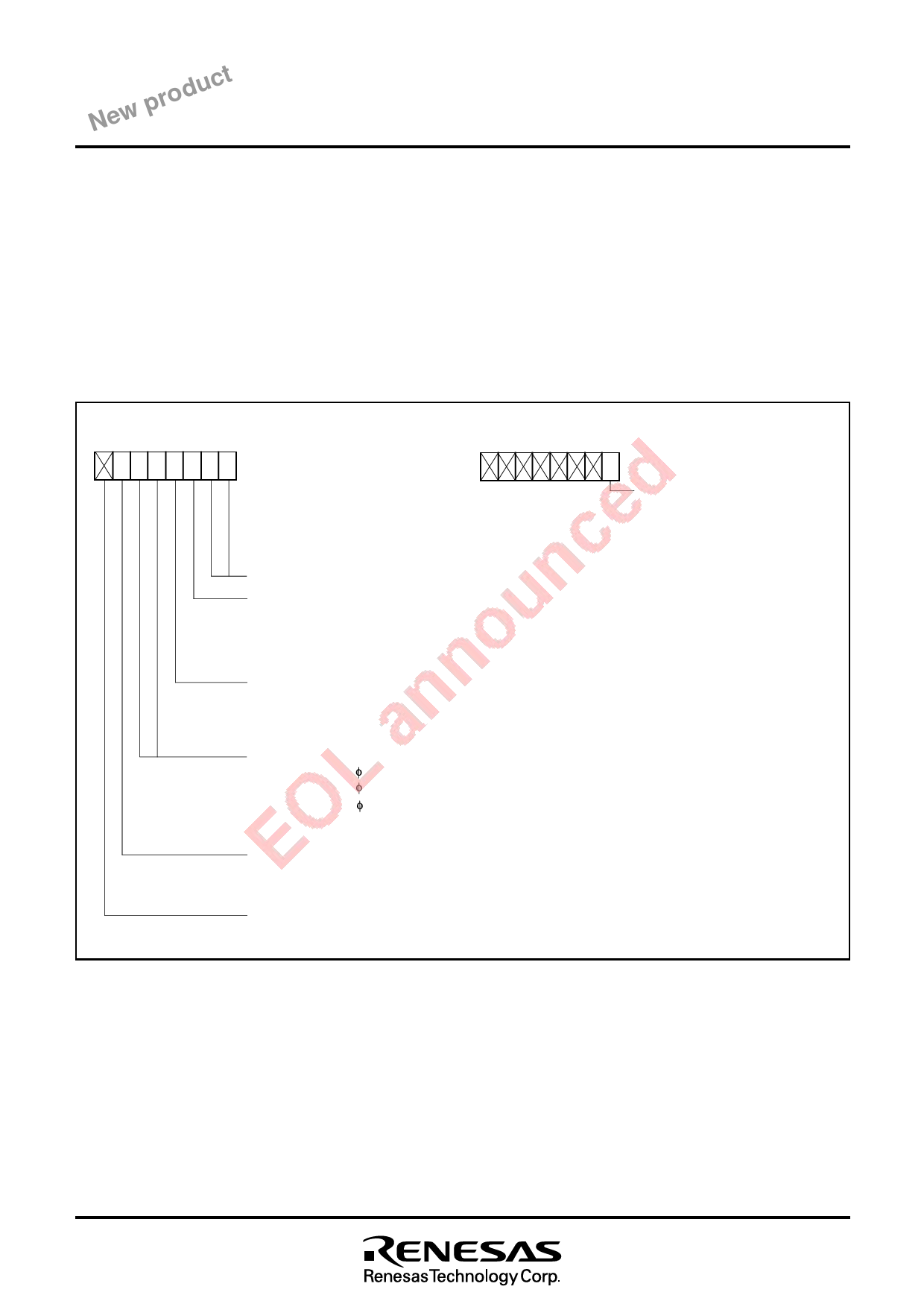
7 654 321 0
Address
0
1 0 Processor mode register 0 5E16
7 654 3210
Address
Processor mode register 1 5F16
Wait selection bit
0 : Wait 0
1 : Wait 1
Must be “10” (“10” after reset)
Wait bit
0 : Wait
1 : No wait
Software reset bit
Reset occurs when this bit is set to “1”
Interrupt priority detection time selection bit
0 0 : Internal clock ! 7 (cycle)
0 1 : Internal clock ! 4 (cycle)
1 0 : Internal clock ! 2 (cycle)
Must be “0”
Not used
Fig. 8 Processor mode register bit configuration
10
Share Link: 