M2V56S20TP Ver la hoja de datos (PDF) - Mitsumi
Número de pieza
componentes Descripción
Fabricante
M2V56S20TP Datasheet PDF : 49 Pages
| |||
SDRAM (Rev.1.1)
Single Data Rate
Feb.2000
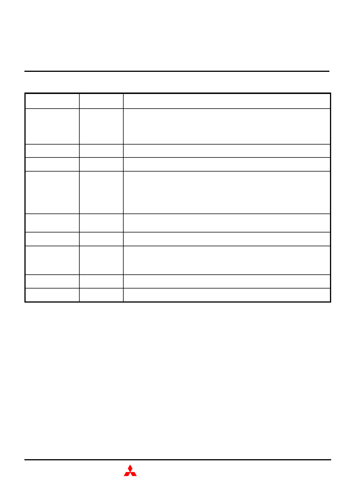
PIN FUNCTION
MITSUBISHI LSIs
M2V56S20/ 30/ 40/ TP -6, -7, -8
256M Synchronous DRAM
CLK
CKE
Input
Input
Master Clock: All other inputs are referenced to the rising edge of CLK.
Clock Enable: CKE controls internal clock. When CKE is low, internal clock
for the following cycle is ceased. CKE is also used to select auto / self
refresh. After self refresh mode is started, CKE becomes asynchronous
input. Self refresh is maintained as long as CKE is low.
/CS
Input
Chip Select: When /CS is high, any command means No Operation.
/RAS, /CAS, /WE
A0-12
BA0,1
DQ0-15
Input
Combination of /RAS, /CAS, /WE defines basic commands.
Input
Input
A0-12 specify the Row / Column Address in conjunction with BA0,1. The
Row Address is specified by A0-12. The Column Address is specified by
A0-9,11. A10 is also used to indicate precharge option. When A10 is
high at a read / write command, an auto precharge is performed. When
A10 is high at a precharge command, all banks are precharged.
Bank Address: BA0,1 specifies one of four banks to which a command is
applied. BA0,1 must be set with ACT, PRE, READ, WRITE commands.
Input / Output Data In and Data out are referenced to the rising edge of CLK.
DQM
DQMU/L
Vdd, Vss
Input
Power Supply
Din Mask / Output Disable: When DQMU/L is high in burst write, Din for
the current cycle is masked. When DQMU/L is high in burst read, Dout is
disabled at the next but one cycle.
Power Supply for the memory array and peripheral circuitry.
VddQ, VssQ
Power Supply VddQ and VssQ are supplied to the Output Buffers only.
MITSUBISHI ELECTRIC
4
Share Link: 