M28W320BB Ver la hoja de datos (PDF) - STMicroelectronics
Número de pieza
componentes Descripción
Fabricante
M28W320BB Datasheet PDF : 43 Pages
| |||
M28W320BT, M28W320BB
SUMMARY DESCRIPTION
The M28W320B is a 32 Mbit (2 Mbit x 16) non-vol-
atile Flash memory that can be erased electrically
at the block level and programmed in-system on a
Word-by-Word basis. These operations can be
performed using a single low voltage (2.7 to 3.6V)
supply. VDDQ allows to drive the I/O pin down to
1.65V. An optional 12V VPP power supply is pro-
vided to speed up customer programming.
The device features an asymmetrical blocked ar-
chitecture. The M28W320B has an array of 71
blocks: 8 Parameter Blocks of 4 KWord and 63
Main Blocks of 32 KWord. M28W320BT has the
Parameter Blocks at the top of the memory ad-
dress space while the M28W320BB locates the
Parameter Blocks starting from the bottom. The
memory maps are shown in Figure 5, Block Ad-
dresses.
Parameter blocks 0 and 1 can be protected from
accidental programming or erasure. Each block
can be erased separately. Erase can be suspend-
ed in order to perform either read or program in
any other block and then resumed. Program can
be suspended to read data in any other block and
then resumed. Each block can be programmed
and erased over 100,000 cycles.
Program and Erase commands are written to the
Command Interface of the memory. An on-chip
Program/Erase Controller takes care of the tim-
ings necessary for program and erase operations.
The end of a program or erase operation can be
detected and any error conditions identified. The
command set required to control the memory is
consistent with JEDEC standards.
The memory is offered in TSOP48 (10 X 20mm),
and TFBGA47 (6.39 x 10.5mm, 0.75mm pitch)
packages and is supplied with all the bits erased
(set to ’1’).
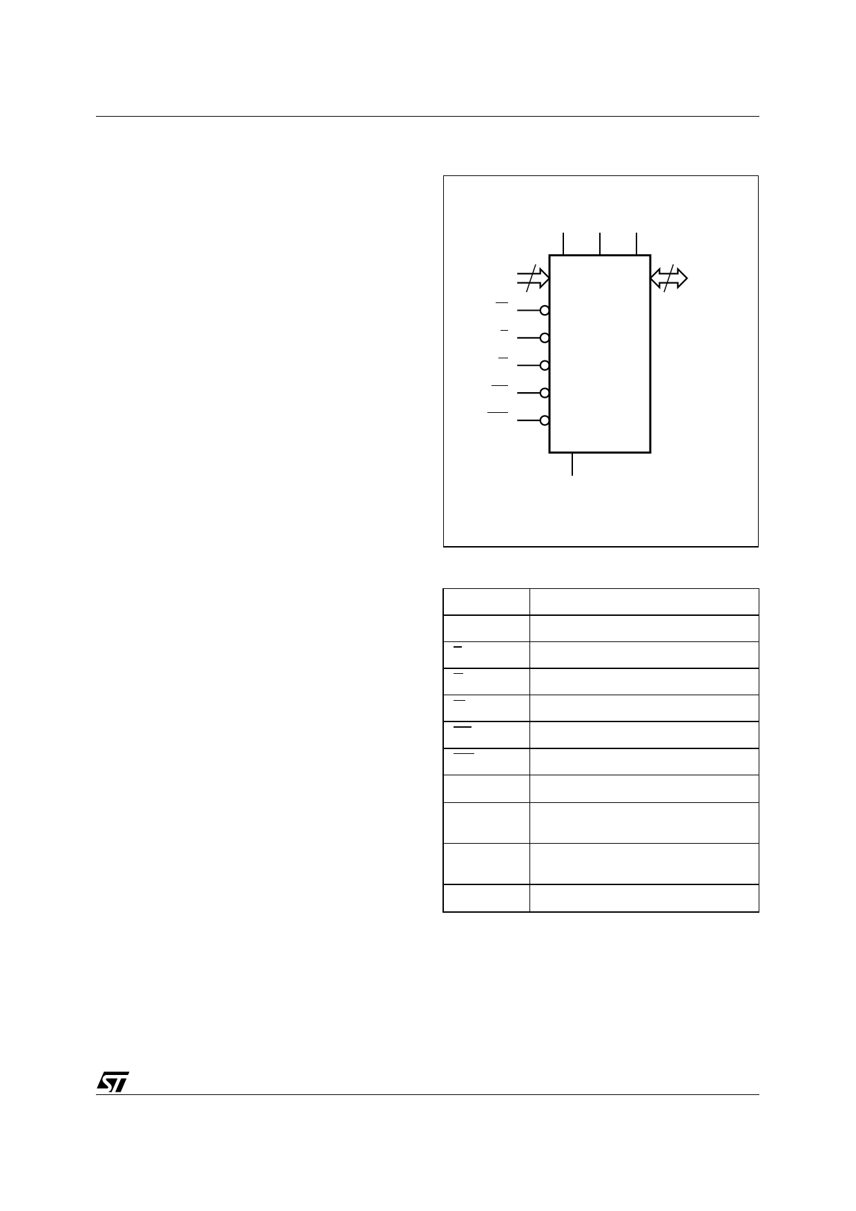
Figure 2. Logic Diagram
VDD VDDQ VPP
21
A0-A20
W
E
G
RP
WP
16
DQ0-DQ15
M28W320BT
M28W320BB
VSS
AI03822
Table 1. Signal Names
A0-A20
Address Inputs
DQ0-DQ15 Data Input/Output
E
Chip Enable
G
Output Enable
W
Write Enable
RP
Reset
WP
Write Protect
VDD
Core Power Supply
VDDQ
Power Supply for
Input/Output
VPP
Optional Supply Voltage for
Fast Program & Erase
VSS
Ground
5/43
Share Link: 